|
60W0_110,EXE Reference Diskette for 5560-W0 v1.10
60W0120R.EXE Reference Diskette for 5560-W0 v1.20
60W111R.EXE Reference Diskette for 5560-W1/W2 (ODP Ready) v1.11
6066B100.zip Reference & Diagnostic Disk for Type-B Upgrade (5560-N) v1.00
80y121r.EXE Reference Diskette for 5580-Y v1.21
80W111R.EXE Reference Diskette for 5580-W (P23T Support) v1.11
80N100.zip Reference & Diagnostic Disk for Type-A Upgrade (5580 & 5560) v1.00
Processor Complex (general info)
Processor Complex Matrix (PS/2 vs. PS/55)
60-W0x Complex
80-Yxx Complex
256K Cache Daughtercard
60-W1x/W2x Complex
80-W0x/W2x Complex
N / DX2/66 Upgrade Type-B Complex
DX2/66 Upgrade Type-A Complex
CPU Upgrades
Complex Upgrades
Content created by Sandy. Edited and new outlines created by Major Tom.
Processor Complex Matrix (PS/2 vs. PS/55)
The following chart was originally presented by Mr. NATICA, one true MCA
enthusiasts from Japan who helped me with my PS/55s in many ways.
Notes:
1) This complex is also called DX2-66 Upgrade Type A.
2) This complex is also called DX2-66 Upgrade Type B. Originally equipped in 60-Nxx.
3) Base clock is 33 MHz but is apparently different from "DX2-66 Upgrade 92F0145" (?).
The 66G1087 and 32G2951 processor boards are unique to the Japanese PS/55 machines.
No direct PS/2 equivalents seems to exist.
Type A can be used both in 5560 and 5580, while Type B can only be used in 5560.
Type 3 and all Type 4 Complexes are commonly used for PS/55 8595-J and PS/2 Model 95.
60 -W0x Complex 486DX 25 MHz, P/N 79F0087, "Corvus"
![[P]](/other/img/photo.gif "Front") |
|
Based on the Type 1 platform. Similar PCB, but not identical.
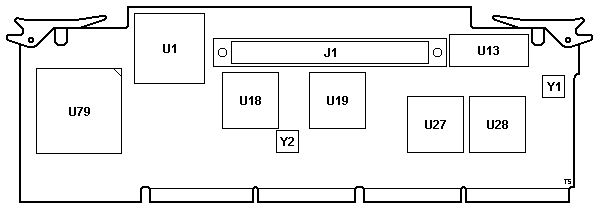
J1 Socket for L2 cache option
U1 57F2194 Memory Controller
U13 79F0181 BIOS ROM
U18,19 78F1659 Data Buffer (RAM)
U27 78F1659 Data Buffer (MCA)
|
U28 90X8134 DMA Controller
U79 169-pin LIF Socket for 486DX-25
Y1 20.0000 MHz osc
Y2 25.0000 MHz osc (CPU)
|
A 256 KB cache daughter board is available as an option.
No Weitek socket, no solder pads.
The board P/N is different from the 80-Yxx complex, but all parts and chips
are the same, except for the oscillator.
This complex can take a 31(?) MHz oscillator without changing the BIOS.
80-Yxx Processor Complex 486DX 33 MHz, P/N 79F2458, "Albireo"
Based on the Type 1 platform. Similar PCB, but not identical.
J1 Socket for L2 cache option
U1 57F2194 Memory Controller
U13 79F0181 BIOS ROM
U18,19 78F1659 Data Buffer (RAM)
U27 78F1659 Data Buffer (MCA)
|
U28 90X8134 DMA Controller
U79 169-pin LIF Socket for 486DX-33
Y1 20.0000 MHz osc
Y2 33.0000 MHz osc (CPU)
|
No Weitek socket, no solder pads.
The board P/N is different from the 60-W0x complex, but all parts and chips
are the same, except for the oscillator.
Memory count is very slow, like the 5561-W0x complex.
Easy to upgrade with DX2-66. You can also use DX4-100, AMD 5x86-133, or
Cyrix 5x86-100 together with an interposer.
A 256 KB cache daughter board is available (see below).
256K Cache Daughtercard P/N 79F1293 or 79F1294? (for 80Y)
The PS/2 Type 1 complex uses a different 17 ns cache module (64F0199).
79F1293 Front
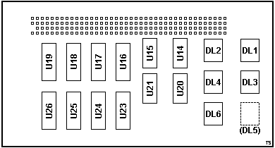
DL1,6 TFF-25 25 ns delay line
DL2,4 TFF-45 45 ns delay line
DL3 TFF-30 30 ns delay line
|
(DL5) Spare
U14,15,20,21 NPC SC47646S (74FCT646)
U16-19,23-26 TC55329J-17 32Kx9 SRAM
|
79F1293 Back
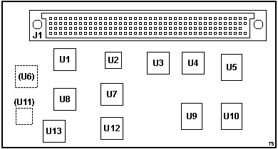
J1 159-pin connector AMP 650754-1
U1 35F3779 PAL
U2 35F3784 PAL
U3 65F1173 PAL
U4 65F1171 PAL
U5,9,10 SN74ACT2160-17FM 8Kx4 TAG RAM
|
(U6) Spare
U7 35F3780 PAL
U8 65F1174 PAL
(U11) Spare
U12 35F3782 PAL
U13 65F1172 PAL
|
60-W1x/W2x Complex 486SX 25 MHz / 486DX2 50 MHz (P/N 07G0460?) "Sofia 2.1"
80-W0x/W2x Complex 486SX 25 MHz / 486DX2 50 MHz (REA 19602276?) "Canberra 2.1"
FRU P/N 95F4299, P/N 07G3153, FCC ID ANOIBM486SXB25
|
|
Same as the Type 2 H/L boards,
including the 07G0463
BIOS ROM.
Important: The original electrolytic SMD capacitors
are prone to leaking! If your board is affected by this problem, you should
replace the capacitors and clean the board as soon as possible. Otherwise, the
leaking electrolyte will inevitably destroy the board!
All 9 SMD capacitors are of the same type - 22 µF 25 V (d = 6.3 mm).
It's safe to use 16 V parts. Polymer or tantalum capacitors can be used as
an alternative.
Memory count is faster than with the 60-W0x complex.
Installed Processor(s)
5580-W0x, 5561-W1x:
5580-W2x, 5561-W2x:
- Earlier models shipped with i486SX-25 in U8 + ODPDX2-50 (ID#06G7015) in U9.
- Later models shipped with just 486DX2-50 in U9.
Reference Disk
Requires system specific ref/diag disks. 5580-W disks on Model 5580, and 5560
-W1/W2 disks on Model 5560.
I got the following message when creating a reference diskette for this model:
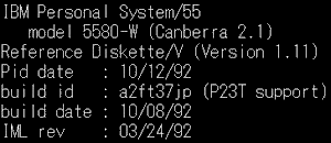
Could "Canberra" be a code name for the 5580-W? See HERE.
"P23T" is 486 OverDrive Processor (ODP).
DMA Controller
Some Type 2 boards suffer from "an incompetent DMA-chip", more info
HERE.
The Japanese "KIT-W2B" has the "bad" 92F1428 DMA chip, yet it works fine with
the following CPUs:
- DX4ODP-75 with 486SX-25 in the 1st socket.
- DX2-66 alone in the 2nd socket (50 MHz internal clock) (huh?)
- DX4-100 on an interposer with VRM, alone in the 2nd socket.
- AMD 5x86 or Cyrix 5x86 (with voltage interposer) in the 2nd socket.
There is no significant difference between the Type 2 "H" and the PS/55 -W1/W2
complexes. Just the board P/N (or FRU?) and BIOS P/N are different.
60-W2 Identification
My machine is labeled as "5561-W1B" and has a "KIT-W2B" sticker.
The area where P/N is silk screened on the -W1 complex is covered with a
"P/N 07G3153" (+ REA number) sticker. There is also a "MPU Upgrade" sticker
stuck to one of the blue lock/release levers.
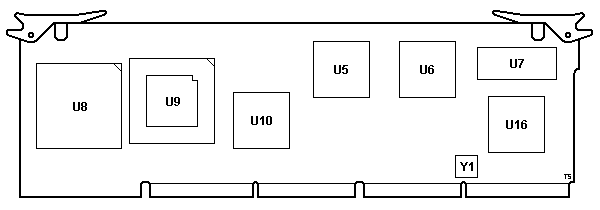
N / DX2-66 Upgrade Type-B Complex FRU P/N 35G2765, P/N 35G2951
|
Based on the Type 2 platform. Similar PCB, but not identical.
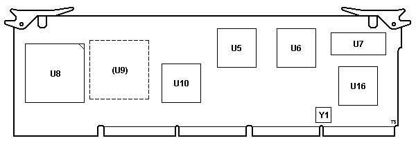
U5 (GA-J) 89F5724 Memory Controller
U6 (GA-M) DMA Controller
U7 35G2957 BIOS ROM
U8 169-pin LIF Socket for 486DX2-66
|
U9 Solder pads for 487 Socket
U10 (GA-T) 64F8781 Memory Data Buffer
U16 (GA-R) 89F5415 MCA Buffer/Controller?
Y1 66.6666 MHz osc
|
U6 The DMA controller chip (U6) is 34G3517
for N, and 92F1428 for W1/2.
Important: The original electrolytic SMD capacitors
are prone to leaking! If your board is affected by this problem, you should
replace the capacitors and clean the board as soon as possible. Otherwise the
leaking electrolyte will inevitably destroy the board!
All 9 SMD capacitors are of the same type - 22 µF 25 V (d = 6.3 mm).
It's safe to use 16 V parts. Polymer or tantalum capacitors can be used as
an alternative.
Originally shipped with Model 5560-N which was introduced to the market in Sep.
1992.
There are at least 2 versions of this complex. While replacing the original
oscillator with a 80 MHz one, I've noticed that some of the PCB traces near the
oscillator were different. I've also noticed an SMD resistor that is not present
on the other board. Both complexes worked fine with the 80 MHz OSC and modified
BIOS ROM.
DX2-66 Upgrade Type-A Complex FRU P/N 66G1106, P/N 66G1088
|
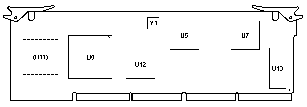
U5 (PA2) 59G1883 SYS#1?
U7 (DMA32) 10G7808
U9 169-pin LIF Socket for 486DX2-66
U11 Solder pads for QFP CPU
|
U12 (PF2) 59G1885 SYS#2?
U13 66G1095 BIOS ROM
Y1 66.666 MHz osc
|
This complex uses the same core logic as the
PS/2 Model 85 "X" and
PS/55 Model 5551-N/Y.
Important: The original electrolytic SMD capacitors
are prone to leaking! If your board is affected by this problem, you should
replace the capacitors and clean the board as soon as possible. Otherwise the
leaking electrolyte will inevitably destroy the board!
All 9 SMD capacitors are of the same type - 22 µF 25 V (d = 6.3 mm).
It's safe to use 16 V parts. Polymer or tantalum capacitors can be used as
an alternative.
Memory count is extremely fast. Support for Streaming Data transfers and
for 2.88 MB floppy drives.
CPU Upgrades
For 60-Wxx, DX4ODP-75 can be used. You can use DX4ODP-100 as well, but it will
only run @ 75 MHz.
The N model will take DX4-100, AMD, or Cyrix with an appropriate VRM
interposer that lowers the core voltage to 3.3 - 3.45 V. Since the N complex
has its CPU socket near the front edge, larger heatsinks won't fit. The same is
true for most active coolers as well. But as long as you use the blue plastic air guide
as intended, your CPU should get *enough* airflow from the front intake fan.
Complex Upgrades
5560-W0/W1 can be replaced to -W2 or -N complex.
5560-W2 can be replaced to -N complex.
5560-W1/W2 complexes can be used in 5580. The associated 5560 ref/diag disks
can't be used in this case. The 5580-Wxx ref/diag should be used instead.
5580 with 60-W0 complex with 5580-Y ref/diag → No equivalent model, but works fine.
5580 with 60-W1 complex with 5580-W ref/diag → 5580-W0x
5580 with 60-W2 complex with 5580-W ref/diag → 5580-W2x
|