|
Prototype Delivery and Capture Boards (82750PA/DA?)
ActionMedia Delivery Board and Capture Board (82750PA/DA)
ActionMedia 2 Delivery Board and Capture Option (82750PB/DB)
ActionMedia Evolution
Thanks to Lorenzo Mollicone, I was able to get
evidence of the ActionMedia Prototype and the release
version of the original ActionMedia. The images are not of
uniform quality, and I cannot do a good job of component
ID. The AM boards use a connector similar to that used on
the Video Capture Adapter/A HERE
and MAYBE the same pinout...
ActionMedia Prototype Delivery Board
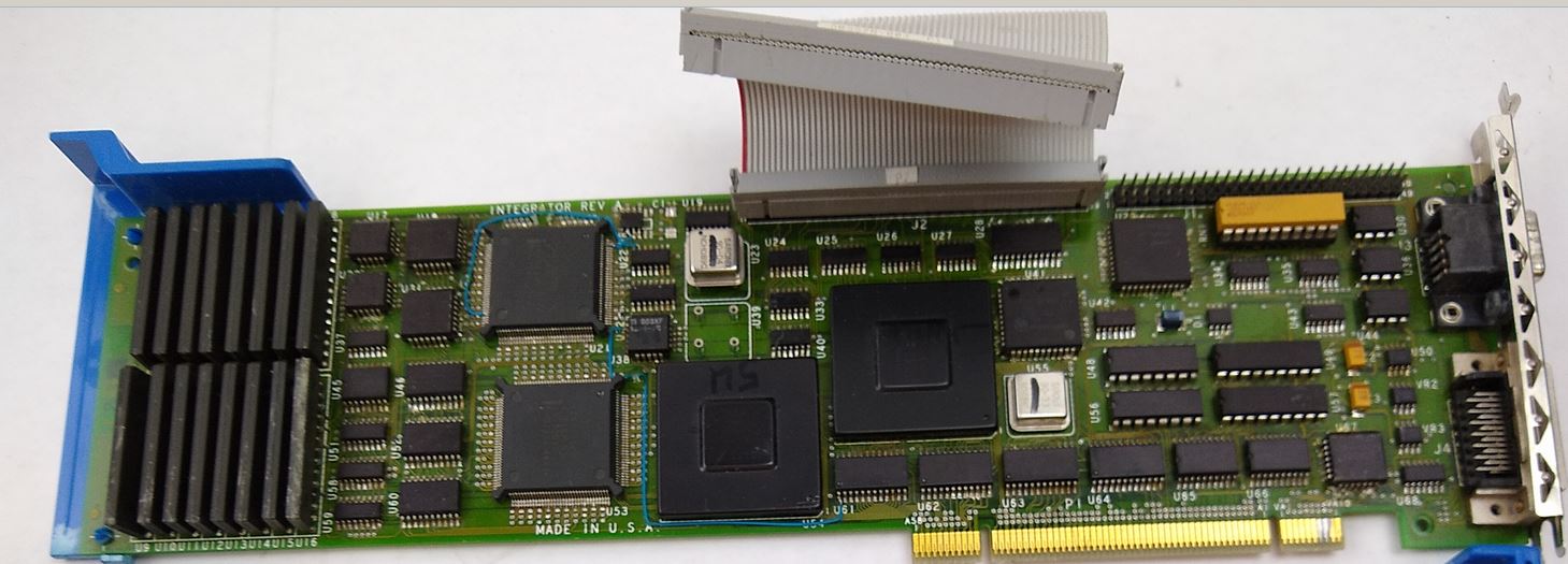
Looks like J1 is for a SCSI controller. It is the 50 pin
header at upper right edge, with the resistor network
below it. The 60 pin header (J2) in the center connects to
the AM Prototype Capture Board below. Most likely card to
card communications. Looks like one of the half-can
oscillators was removed, see the solder tail sockets? See
the AVE connector used to pick up Base Video?
ActionMedia Prototype Capture Board
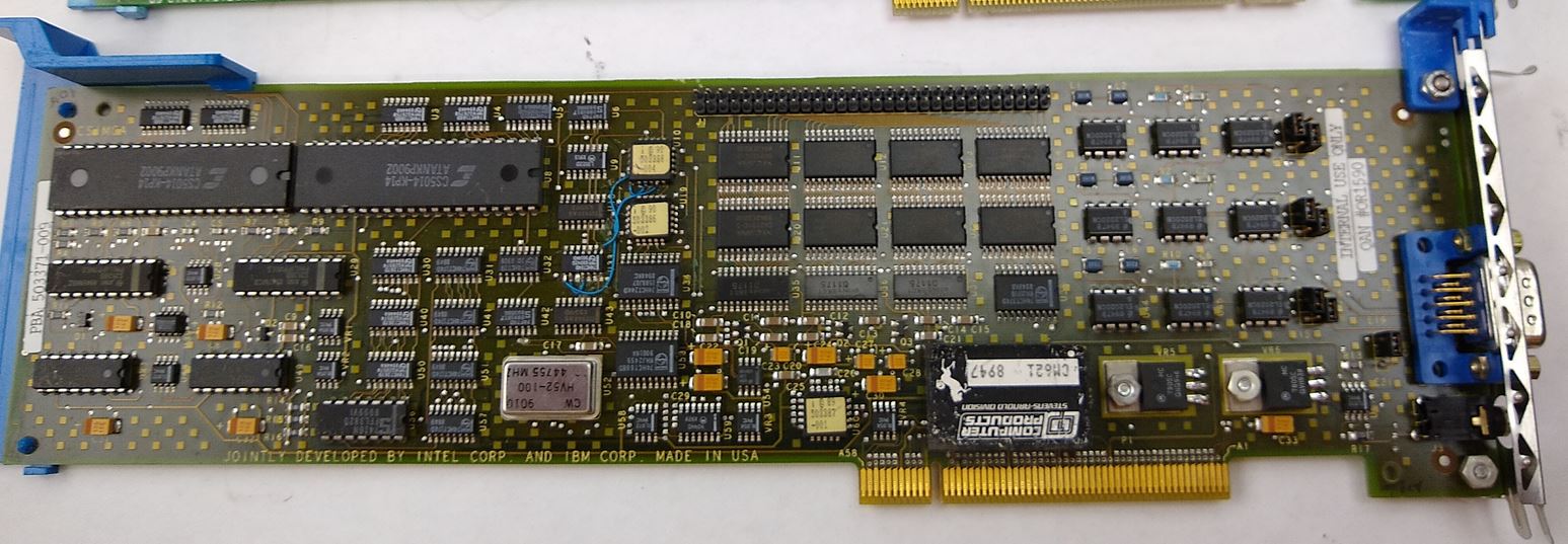
I don't have any pics of the connectors on the brackets,
so if this is a DE9 or HDD15, I can't tell. Notice the 1/8
inch audio jack at the lower right. See the three sets of
six pin headers towards the right side? See the three pin
header to the left of the blue video port? My guess it is
similar to E1 on the AM2, and is used to choose digital
keying over the AVE on the Delivery card, or Analog
keying, via a video cable attached to the video
connector...
Notice the pair of CS5014-KP1A at upper left corner? Full
can oscillator shows a date of 9010. U52 is 12.44755 MHz
(inking indistinct)
ActionMedia Delivery Board
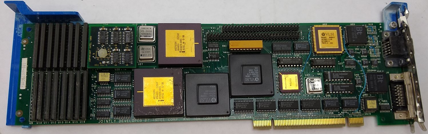
You can see the 82750PA and 82750DA. J1 (50 pin header) is
now at top dead center. J2 (60 pin header) is right below
it. Pair of Bt RAMDACs. I think the date code on the
82750PA is 9044. U18 25.0000 MHz, U27 14.3181 MHz, U47
33.868 ? damaged osc...
ActionMedia 2 Delivery Card w/ Capture Option
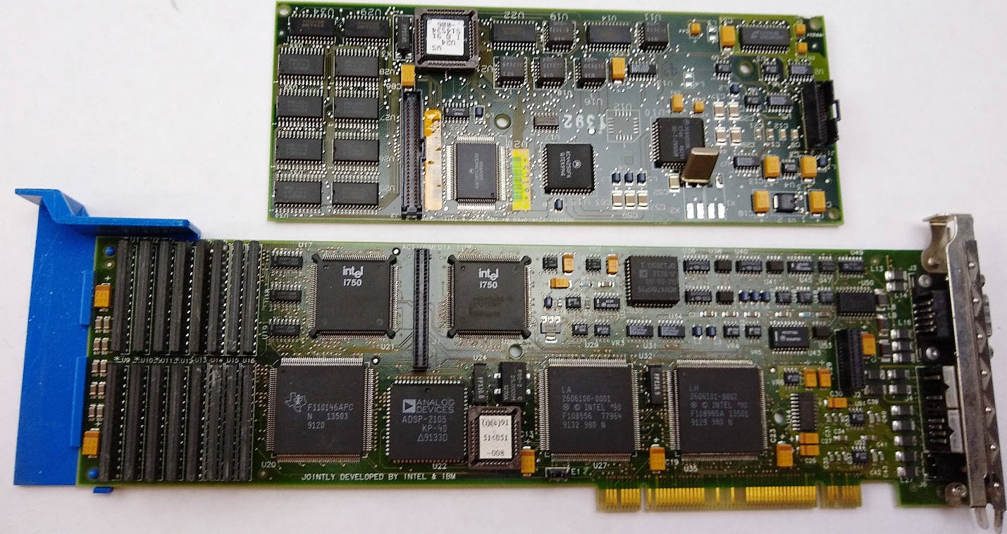
ActionMedia 2 Capture Option (CS2) dated 4791
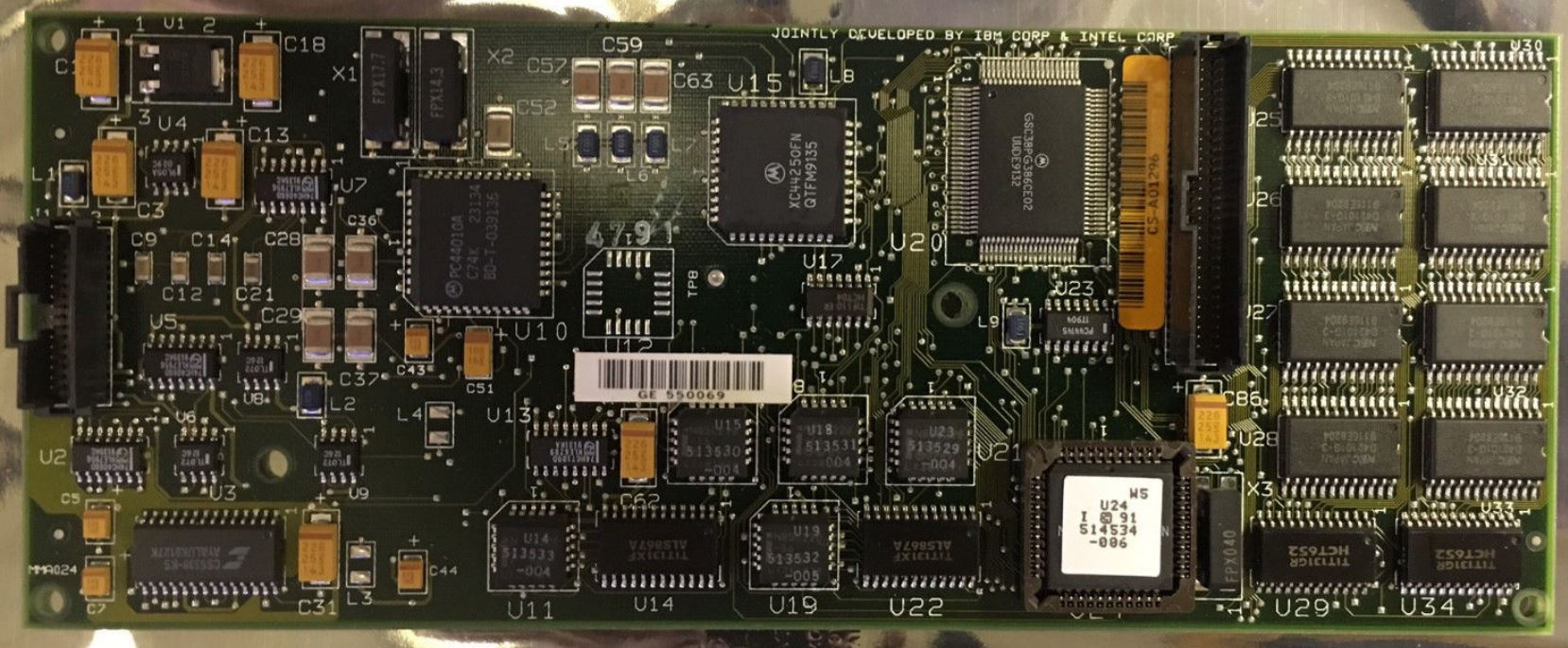
Grabbed this pic from Lorenzo Mollicone and it verifies my
suspicions about X1 and X2. They are SMD xtals. X1 is
FPX17.7 and X2 is FPX14.3 Please note that FPX040 is at
the lower right corner of the socketed PLCC. All versions
of the PLCC are © 91, 514536 -006.
4791 - X1, X2 SMD crystal, four solder pads per xtal.
1292 - X1, X2 radial lead cans, four solder pads per xtal.
Case not soldered to solder pads by edge of PCB. X1 signal
leads doglegged to solder pads.
1194 - X1, X2 xtals same locations, but no solder pads for
xtals. Both signal leads stick straight out to through
holes. Each xtal case is fastened by a single pin to a
through hole.
FPX Case and Side


|