|
rfp70a.exe P70 386 Reference Disk v1.04 (zipped image)
190-053 PS/2 MODEL P70 386 (8573-031)
189-074 PS/2 MODEL P70 386 (8573-061 / 121)
SHS15F2198 IBM PS/2 Model P70 386 HMS
SHS64F3994 IBM PS/2 P70 386 HMR
tpvol1.pdf HMM for IBM PS/2 P70/P75 and laptops/notebooks
S68X-2377-00 IBM Personal System/2 Model P70 Technical Reference Apr 1989
P70 Supplement for the Hardware Interface and BIOS Interface Technical Reference
P70 Transport Brochure (scan by David Beem)
DBA-ESDI Hard Drive Interface
Planar Types
P70 Old System Board
P70 New System Board
System Firmware
ROM Images
Supported Memory
The Mysterious "Masked SIMM" Revealed!
Old Video Card
New Video Card
Plasma Display Adapter Connector ("Display" on planar)
Plasma Connector Pinout
Plasma Display Auto-Dim Block Diagram
Floppy Drive
Floppy Drive Replacement
Support for 2.88MB Floppy Drives on New System Board FRU 56F9085
Remove P70 Floppy (H2)
ALPS DFP723D15C Rear PCB FP1T08D from a sick floppy
Disable ESDI Controller
Derive MCA Bus from ESDI Ports?
Remove Battery
Pointing Device Port (Not for KB!)
305 Error at Power-Up
P70 Drive Carrier Mounting Hole Spacing
Auto 16/4 Token Ring Card Fits Lower Slot
113 Error
Fitting a SCSI hard drive
Early P70s Loose Configuration After Quick On-Off-On
IBM 7186 - GE Fanuc Workmaster II
Planar Types
For the original document, go to Dr Jim's P70
Project.
The P70 came in two planar versions: the older 38F4688/65X1564, used
primarily in the 20 MHz -061 machines (but also seen in some -121 20 MHz
boxes), and the 38F6973/56F9085 used in 16 MHz and 20 MHz -121 models.
38F4688/65X1564 planars have the 386DX socket immediately to the right of
the 387DX socket, and two BIOS ROMs near the upper left edge of the board. The
38F6973/56F9085 has the 386DX socket above and to the left of the 387DX socket.
Another distinguishing feature of the newer models is the inclusion of video
output filtering on the video card instead of on a 'daughter card' fitted in
series with the video output cable. The newer planar seems slightly faster on
some benchmarks, but the difference is hardly noteworthy.
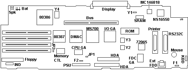
P70 Old System Board "SYS CARD 386" (Japanese design)
16 MHz: "IGH0254EA-A" or "IGH0254FA", FRU P/N 38F5969, P/N 38F7806
![[P]](/other/img/photo.gif "Old 16 MHz Front")
20 MHz: "IGH0254DA-A", FRU P/N 65X1564
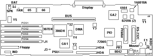
146818A MC146818A RTC
4464 NEC D4464G-15L
65 PN 65X1565
66 PN 65X1566
72065 NEC D72065L
8259A NEC D71059L
8042 IBM MPD80C42C-146
BAT 6V Battery
Bus MCA riser slot
Display 16-bit MCA video slot
DMA 90X8134 DMA Controller
Ext FDD Hosiden connector
F1 KB fuse "SOC 1A"
Fan Solder pads
Floppy 34-pin header
GA1 38F7800
GA2 65X1279
HDA Top 34-pin header
HDA Bottom 40-pin header
IND Indicator header
|
J1 Power On Password
J2 solder pads
J3 solder pads
J4 solder pads
KBD Keyboard header
Mouse Mouse header
PIO 72X8299
POS1-4 72-pin SIMM slots
Printer DB25 port
PRT 94X1265
PSU Power header
RS-232C DB25 serial
SPK Speaker
UART NS16550AFV
Y1 32 KHz xtal
Y2 1.843 MHz osc
Y3 14.31 MHz osc
Y4 40.0000 MHz osc
Y5 32.0000 MHz osc
|
P70 New System Board "SYS CARD DX" (Japanese design) (original scans by Jay P. Thorne)
16 MHz: "IGH 0322DA", FRU P/N 56F9085, P/N 56F7435
72065 NEC D72065L
8042 Outline, not populated
BAT 6V Battery
Bus MCA riser slot
CPU GA 33F5946
Display 16-bit MCA video slot
DMAC 90X8134 DMA Controller
Ext FDD Hosiden connector
Fan Solder pads
F1 KB fuse "SOC 1A"
F2 Fuse "SOC 3A"
FDC GA 33F8602
Floppy 34-pin header
HDA Top 34-pin header
BA Bottom 40-pin header
IND Indicator header
I/O GA 33F5838
J1 solder pads
J2 Power On Password
|
KBD Keyboard header
MC146818 MC146818AFN RTC
Memory Controller GA 33F5944
Mouse Mouse header
MS700 57X4111
NS16550 NS16550AFV
PAL 20L8 marked "ROM"
POS1-4 72-pin SIMM socket
Printer DB25 port
PSU Power header
ROM HN27C301G-20 ROM P/N 56F7439
RS-232C DB25 serial
SPK Speaker
SRAM NEC D4464G-15L
Y1 32.768 KHz xtal
Y2 14.31 MHz osc
Y3 24.000 MHz osc
Y4 40.0000 MHz osc
|
This planar uses the same core logic as the
8570 Type 2 planar, the
5550-S/T Stage 2 planar, and the
Type 0 processor complex.
Odd, the 8259As have been integrated into one of the Gate Arrays. The 8042
has also been integrated, but there is a 8042 PLCC outline to the right of the
PS/2 mouse port. PRT has also disappeared.
System Firmware (POST & BIOS)
Firmware stored in EPROM.
ROM Images
Old Planar (FRU P/N 38F5969 or 65X1564)
38F5957 / 38F5958 * - 16 MHz Planar, 07 Feb 1989, rev. 0, 2x D27512-200V10 (right / left) (thx Mike Lycett)
* board w/ swapped ROM stickers spotted (1 out of 3 samples so far; the affected board came from a GE Fanuc unit)
65X1566 / 65X1565 - 20 MHz Planar, 18 Jan 1989, rev. 0, 2x D27512-200V10 (right / left)
New Planar (FRU P/N 56F9085)
56F7439 - 16 Dec 1989, rev. 1 / 2 *, 1x HN27C301G-20 (not marked)
* reports rev. 1 for 16 MHz systems, rev. 2 for 20 MHz systems
Supported Memory
From Bob Eager:
The P70 has four 72-pin SIMM slots. Unlike the P75, the largest
SIMM that can be used is 2MB. The speed can be 85 ns or 80 ns.
Just like their big brother, the P70 prefers the Panasonic SIMM in SIMM2. 85
ns speed.
SIMM1: 65X6249
SIMM2: 65X1309/FRU 90X8625/iGH0258DA
SIMM3: 65X6249
SIMM4: 65X1309/FRU 90X8625/iGH0258DA
The Mysterious "Masked SIMM" Revealed!
2 MB 85 ns P/N 65X249 - FRU 92F0104
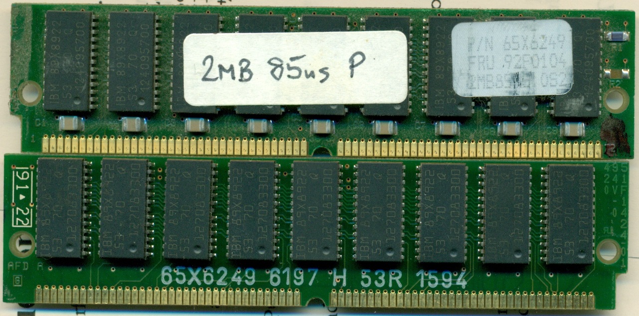
Thanks to Tim N Clarke for digging through his private stash. Notice the
places for R1 and R2, yet there is no solder dots on the reverse for R3 and R4.
Yet the multimeter shows OXOX (pins 67-68-69-70). From this, "masked" probably
means the SIMM's PCB connects pin 68 internally, i.e. in the mask for the
traces.
2 MB 85 ns FRU 90X8625 - P/N 65X1309 - iGH0258DA
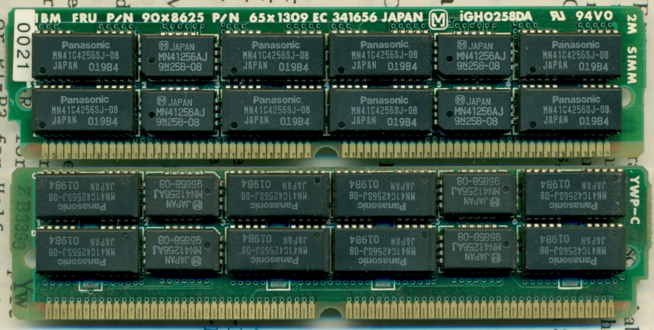
This is an original Panasonic iGH0258DA. Not even markings
for PD resistors. Yet the multimeter shows OXOX (pins
67-68-69-70). PD bit shunts are definitely part of the
SIMM's PCB mask.
Note: the four white outlines under the big
memory chips are SMD capacitors. If you look edge-wise at the SIMM
against the light, you will see SMD caps under the big
chips on BOTH sides..
Kingston KTM-2000/M70 Failures
The P75 will digest Kingston KTM-2000/M70 memory, but the late P70 planar
wants nothing to do with it. When I was trying to snap a KTM-2000/M70 into the
socket, it looked "bowed", it may be the center notch is not deep enough? I
kept getting not properly seated as a possible cause.
But whether it was all KTM-2000/M70, or M70/IBM, it threw a 225.
Peter said:
I cannot recall right from out of my head if the P70 reads all 4
bits of the PD signal or if it masks it down to the two important bits only. In
this case certain 4MB modules might be detected as 2MB... but end up in an
error later during memory count.
Old System Display Card
"DISP CARD(P/GA)", "iGH0253BA", FRU P/N 38F4686, P/N 38F5942 (Japanese design)
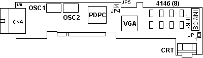
41464x8 HM50464CP-12 64Kx4 DRAM
CN4 26-pin plasma display header
CRT HDD15 video connector
INMOS IMG171P-35 RAMDAC
OSC1 25.175 MHz osc (shielded)
OSC2 28.322 MHz osc (shielded)
JP1 2-pin jumper Unk (not set)
|
JP2 2-pin jumper Unk (not set)
JP3 2-pin jumper Unk (not set)
JP4 3-pin jumper Unk (2-3 set)
JP5 3-pin jumper Unk (1-2 set)
JP6 2-pin jumper Unk (not set)
PDPC 65X1331
VGA 90X8941
|
The PDPC hooks to the same signals as
the INMOS RAMDAC — specifically
D0-D7, P0-7, PCLK, -BLANK, and possibly more. It then processes these signals
and generates additional signals required by the plasma display.
New System Display Card "DISP CARD (GA)", "iGH0334DA", FRU P/N 38F4686, P/N 38F7793 (Japanese Design)
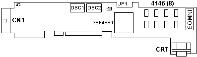
Features a single IBM ASIC - 38F4681.
Arne Falch wrote:
By the way, I have the new type of display card and plasma panel.
Since the old display card will not work with new plasma panel (or vice versa),
I guess that the old panel connections are different. The panel is a Matsushita
electric type MD480T640PG4, P/N 38F4744. made in week 06, 1990.
The machine is originally a model 8573-031 (16 MHz processor, 30 MB disk),
but someone has put in a 60 MB disk.
Graphics (from Peter)
The VGA port supports all VGA graphics and text modes including 640 x 480
graphics, 320 x 200 graphics in 256 colors, and 720 x 400 text using any
optional PS/2 VGA color display, and maintains compatibility with CGA and EGA
modes. Unlike to the P75 the P70 cannot drive Plasma and external VGA at one
time - except in DIAGS mode.
As I said in a previous posting: the VGA chipset on the plasma-video adapter
is the same 256K-IBM / INMOS stuff as used in the Mod. 50 / 60 / 70 / 80 - and
therefore has the same limits: 640 x 480 at 16 colours ... ending of sending.
So the answer is "No - you cannot get more colours at 640x480".
I'd really tried a lot to get more out of that thing (back in the good old
days) but it simply doesn't work. The available memory on the bit-planes is too
low. You need at least 512K VRAM (and a better Video DAC) but the Inmos DAC
*should* be able to get it - probably. It is specified for a video bandwidth of
18.44 MHz only (which is 640 x 480 with 60 Hz vertical refresh) - but the main
problem is the missing Video-BIOS mode for 256 colours at 640 x 480 and the
missing V-RAM.
Simple calculation: 640 x 480 pixels = 307.200 pixels total. Each one
occupies 4 bit for 16 colours = 153.600 bytes V-RAM (Video Mode 12h). The 320 x
200 / 256-colour mode (Mode 13h) occupies 8 bit per pixel and therefore a
256-colors mode would need double the space.
The Video-DAC controls 4 x 64K for each "Map", where the maps are the
bit-planes for red, green, blue and intensity on the 640 x 480 mode. The
Video-DAC adress buffer resides at A000h - AFFFh (whereas the locations from
A95FF - AFFF are "reserved").
I really tried to write a video driver for this thing ... but it is hard to
replace hardware with software - especially if you have the hardware missing to
support that. :-D
>is possible to use the display card of a P/2 Model P70 in another PS/2
system with onboard VGA. I don't want to use both screens in the same time. I
do not want to use any CRT. I want to use the plasma screen on my PS/2 Model
55.
As far as I can tell - you can't. The plasma board is basically a plain
vanilla VGA card with a different output stage for the row/column addressing of
a plasma display. But internally it uses the same chips, addresses and ports
like the generic onboard VGA of the 55SX - apart from the odd form-factor of
this card.
The card-ID should be EDAF - but there is no ADF for this card. There is an
@EDAF.DGS on the P70 reference and that means the ADF function is substituted
by the board logic setup internally, so you cannot take it over anyway.
The P70 / P75 have built-in information on this EDAF card and need no ADF
then - the 55SX (and none of the "normal" PS/2 machines) hasn't. In addition
you need the P70 power supply for the high voltages to run the plasma
display.
Plasma Display Adapter Connector
The following table shows the signal assignment of the plasma display
adapter MCA connector. The connector features the same signal set as the 16-bit
Micro Channel connector (see HERE) except
for two pins. The pin B04 does not provide the 14.3 MHz clock signal and the
pin B45 carries the signal -KEYSTROKE for the plasma display.
| Pin | Signal | | Pin | Signal |
|---|
| B01 | AUDIO GND | A01 | -CD SETUP |
| B02 | AUDIO | A02 | MADE 24 |
| B03 | GND | A03 | GND |
| B04 | Reserved* | A04 | A 11 |
| B05 | GND | A05 | A 10 |
| B06 | A 23 | A06 | A 09 |
| B07 | A 22 | A07 | +5 Vdc |
| B08 | A 21 | A08 | A 08 |
| B09 | GND | A09 | A 07 |
| B10 | A 20 | A10 | A 06 |
| B11 | A 19 | A11 | +5 Vdc |
| B12 | A 18 | A12 | A 05 |
| B13 | GND | A13 | A 04 |
| B14 | A 17 | A14 | A 03 |
| B15 | A 16 | A15 | +5 Vdc |
| B16 | A 15 | A16 | A 02 |
| B17 | GND | A17 | A 01 |
| B18 | A 14 | A18 | A 00 |
| B19 | A 13 | A19 | +12 Vdc |
| B20 | A 12 | A20 | -ADL |
| B21 | GND | A21 | -PREEMPT |
| B22 | -IRQ 09 | A22 | -BURST |
| B23 | -IRQ 03 | A23 | -12 Vdc |
| B24 | -IRQ 04 | A24 | ARB 00 |
| B25 | GND | A25 | ARB 01 |
| B26 | -IRQ 05 | A26 | ARB 02 |
| B27 | -IRQ 06 | A27 | -12 Vdc |
| B28 | -IRQ 07 | A28 | ARB 03 |
| B29 | GND | A29 | ARB/-GNT |
| B30 | Reserved | A30 | -TC |
| B31 | Reserved | A31 | +5 Vdc |
| B32 | -CHCK | A32 | -S0 |
| B33 | GND | A33 | -S1 |
| B34 | -CMD | A34 | M/-IO |
| B35 | CHRDYRTN | A35 | +12 Vdc |
| B36 | -CD SFDBK | A36 | CD CHRDY |
| B37 | GND | A37 | D 00 |
| B38 | D 01 | A38 | D 02 |
| B39 | D 03 | A39 | +5 Vdc |
| B40 | D 04 | A40 | D 05 |
| B41 | GND | A41 | D 06 |
| B42 | CHRESET | A42 | D 07 |
| B43 | Reserved | A43 | GND |
| B44 | Reserved | A44 | -DS 16 RTN |
| B45 | -KEYSTROKE* | A45 | -REFRESH |
| B46 | PHYSICAL KEY | A46 | PHYSICAL KEY |
| B47 | PHYSICAL KEY | A47 | PHYSICAL KEY |
| B48 | D 08 | A48 | +5 Vdc |
| B49 | D 09 | A49 | D 10 |
| B50 | GND | A50 | D 11 |
| B51 | D 12 | A51 | D 13 |
| B52 | D 14 | A52 | +12 Vdc |
| B53 | D 15 | A53 | Reserved |
| B54 | GND | A54 | -SBHE |
| B55 | -IRQ 10 | A55 | -CD DS 16 |
| B56 | -IRQ 11 | A56 | +5 Vdc |
| B57 | -IRQ 12 | A57 | -IRQ 14 |
| B58 | GND | A58 | -IRQ 15 |
Plasma Display Connector
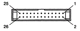
| Pin | Dir | Signal | Pin | Dir | Signal |
|---|
| 1 | O | -Vsync | 2 | — | Ground |
| 3 | O | -Hsync | 4 | — | Ground |
| 5 | O | -Data 0 | 6 | — | Ground |
| 7 | O | -Data 1 | 8 | — | Ground |
| 9 | O | -Data 2 | 10 | — | Ground |
| 11 | O | -Data 3 | 12 | — | Ground |
| 13 | O | -Display Timing | 14 | — | Ground |
| 15 | O | -Dot Clock | 16 | — | Ground |
| 17 | O | +Disable | 18 | — | Ground |
| 19 | O | -Blanking | 20 | — | Ground |
| 21 | O | -Gamma Compensation | 22 | O | -Background Intensity |
| 23 | — | Ground | 24 | — | Ground |
| 25 | — | Ground | 26 | — | Ground |
Arne Falch wrote regarding the "new" display adapter (edited):
I used a scope on the connections, and I was able to identify pins
for 4 databits, pixel clock, vertical and horizontal sync. There are still 2 or
3 unknown signal pins, one is probably a blanking or data enable pin.
1 - Vertical sync, active high. 15 ms period, 62 us high pulse.
3 - Horizontal sync, active low. 32 us period, 3.8 us low pulse.
5,7,9,11 - Pixel Data
13 - Data Enable? One long 8 ms high pulse, then many 32 us period pulses, with
high time = 6.3 us. Then pattern repeats.
15 - Display Data clock. Approx. 40 ns period, my guess is frequency is the
same as one of the oscillators. (Ed. 4x10^8 inverse
is 25 MHz)
17 - Display On/Off. Low signal = on. Goes high after 10 min display blanking
timeout.
19 - Blanking. 1.1 ms low, 2.7 ms high, 1.1 ms low, 11 ms high, then pattern
repeats. Maybe the 1.1 ms periods is longer when the display is blanked at the
top/bottom in CGA/EGA mode? I will look into this when I get software that
enables CGA/EGA mode.
21 - Unknown signal. No visible activity.
Signal connections:
1 - Pin 16 on 74LS241 via 330 ohm
3 - Pin 18 on 74LS241 via 330 ohm
5,7,9,11,13,17,19 - 38F4681 ASIC
15 - 38F4681 ASIC; goes to a pin with GND pins on both adjacent pins
- this corresponds well with a clock signal
21 - No visible activity
P70 Auto Dim Block Diagram
Auto-dim function:
The plasma display has an auto-dim function. It automatically
turns the plasma display off after the specified period since the last
keystroke. Any keystroke returns the plasma display on.
A desired value for
the period can be specified approximately in the range 1 to 120 minutes during
the system configuration by the backup copy of the reference diskette.
Note: For German models, the background intensity
of the screen is selectable. The background intensity does not affect the
auto-dim function.
The auto-dim logic is integrated in the PDC on the adapter card. (See Figure
4-3.)
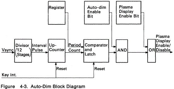
The sequence of auto-dim operation is as follows. (See Figure 4-3.)
- During the system configuration, plasma display may be enabled (PDP ENABLE
bit is set) and a value corresponding to the specified period is stored.
- When the auto-dim function is enabled. the AUTO-DIM ENABLE bit is set by
POST (Power-on Self Test).
- The up-counter increases each minute with a interval pulse derived from the
VSYNC (Vertical Synchronization) signal.
- The comparator compares the count and the value specified for the period,
then the result is latched.
- The result is gated twice into the plasma display.
If the AUTO-DIM ENABLE bit is set and the count has reached the matching value,
the plasma display is disabled and the up-counter is reset. Otherwise, nothing
is performed.
- Go to step 3.
Floppy Drive
P70 comes with ALPS DFP723D15B 3.5" 1.44 MB floppy drive. FRU 38F5936
Floppy Drive Replacement
From Bob Eager:
The diskette drives on these machines suffer badly from the
ingress of dirt and dust, mainly due to the orientation of the drive. The head
mechanism also has to push the heads up against gravity, which causes excessive
actuator spindle wear. Both of these can cause slow response to the Power On
System Test (POST), generating errors such as 601 (diskette drive failure) or
162 (configuration error due to the failure of the drive to be detected).
The correct FRU number for a replacement diskette drive is FRU 38F5936.
However, it seems that FRU 64F0162 will also fit, and is electrically
compatible. This drive is commonly used in the following machines: Model 55SX
(8555), Model 60 (8560), Model 65SX (8565) and Model 80 (8580). It is also used
in some Model 85 (9585), Model 90 (8590) and Model 95 (8595) systems, except of
course when a 2.88MB drive is fitted! Note that the 8560, 8565 and 8580 have
also used a different drive with a 40 pin card edge connector rather than the
34 pin header; this will not fit. In all cases, it will be necessary
to remove the plastic drive sled from the base before fitting the drive to a
P70. The blue plastic button may be a different length, so it may be a good
idea to keep the button from the old drive (it simply pulls off) to fit to the
replacement drive.
Floppy Drive Adapter
Adapter designed to allow replacing a failed IBM P70/75 drive with a
standard PC floppy drive:
IBM PS/2 P7X Floppy Drive Adapter (by Malte Dehling, GitHub)
Support for 2.88MB Floppy Drives on New System Board FRU 56F9085
While desperately searching for a working drive, research turned up some
assertions that the 2.88MB 64F4148 worked (Sony MP-F40W-00). The floppy header
is on the correct side, the only downside is that the floppy eject button is
about 1/8" too long to shut when a floppy is in the drive. Not a bad
trade-off.
I dunno, maybe the FDC Gate Array adds functionality to the NEC D72065L. But
the new planar does support the 2.88MB under the original Refdisk (at what
capacity I dunno). If you patch the original Refdisk with XGAOPT it updates some things...
End result is a choice for 2.88MB Diskette. Note that running
autoconfiguration sets it to 1.44MB, but hey, it still works!
Remove P70 Floppy
(I have two -121s, one has the H1, the other has an H2.)
Remove Floppy (H1)
Remove Floppy (H2)
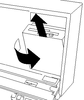
Open the plasma screen so you can get your hand behind it.Grasp the lower
edge of the drive cover, pull out and forward. Once it snaps off (you will feel
it, pull the cover up and out. If you grab onto the floppy slot, it should give
you enough of a grip to do it.
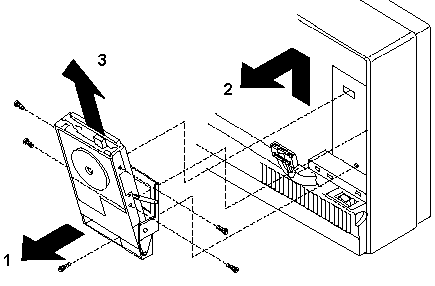
Unscrew the black screw at the bottom center of the drive carrier. If you
look between the floppy cable and the grounding strap, you will see it. Thank
God it's a captive screw. It's a combo standard/phillips screw.
With the retaining screw loose, push the drive carrier up until it comes
free of the case clips. Now you have full access to the floppy drive mounting
screws.You must remove the floppy from the carrier before you can take the
floppy cable out.
Install Drive Carrier
Reverse action of removal. Hook on case clips and pull down. When
seated, screw in the black retaining screw in the bottom center. Now look at
the sides of the drive carrier. Notice the slots about half way up the carrier-
they go straight in, then go down. Look at the cover- it has two posts... slide
the cover onto the carrier, make sure the eject button is lined up with the
hole. Now push the cover down until it snaps into place. Congratulations, break
out the Jolt!
ALPS DFP723D15C Rear PCB FP1T08D
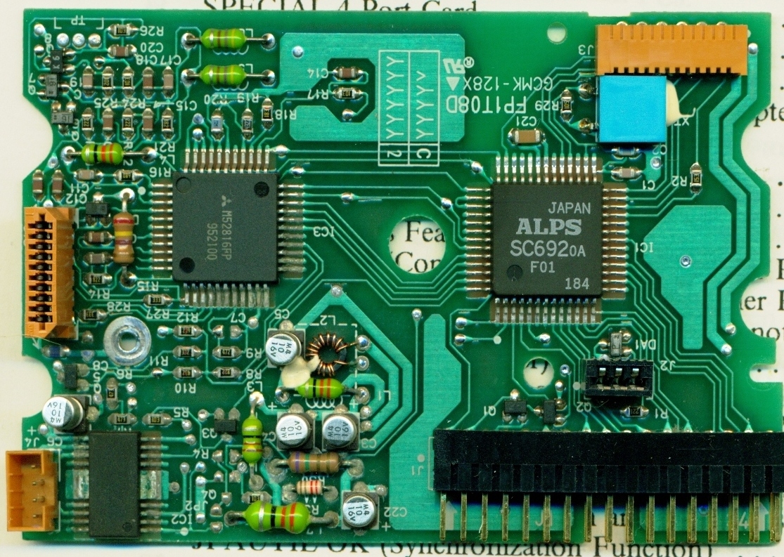
The image is of the rear or bottom PCB from an ALPS DFP723D15C floppy drive,
P/N 38F7802 FRU 38F5936. It is correctly oriented in the position it would be
when installed, e.g. with the 34 pin header pointed down.
Not a fun day. Many of the solder joints in the lower left have a "grainy"
look to them. Oddly enough, the power component in the lower left corner by J4
(floppy motor power) has green corrosion on BOTH sides. One would think if it
was from a leaking cap, it would be toward the source of contamination.
At this point, I am hesitant to start recapping, due to the poor looking
solder joints of a whole bunch of teeny tiny components. Heck, some SMD
components have the grainy solder appearance looking almost as big as the
component... Maybe a good application of baking soda and water could remove
some of this, but I am not confident.
Disable ESDI Controller
>I will be surprised if it can be disabled.
Peter said:
Just remove the harddisk... the ESDI controller is underside :-)
These drives are drive and controller in one physical unit. The strange
2-connector port they are attached on the P70 is in fact a "sort of" MCA
connector. The card-ID is DF9F and it will show up at slot 3 in the setup.
MCA Bus from ESDI Port?
> Can you hack an MCA bus out of the pseudo-one in the ESDI-DBA
connector?
Ed Avis replies:
I'm told that this is not possible because the connector carries
only those signals needed for the disk, and not enough for a general MCA
card.
Remove Battery
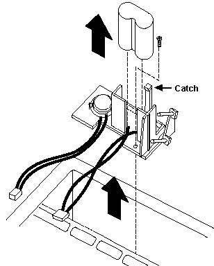
|
This shows how to remove the carrier and battery. To replace just the
battery, pull the catch away from the battery, and pull the battery up. Battery
is FRU 72X8498. Usually in the
camera section of your local supermarket.
|
Pointing Device Port (or Mouse Port)
Peter says:
The rear port is designed 'pointing device port' in users manual
as well as HMM. No keyboard will work on this port ! Don't use a serial mouse
to PS/2 port adapter! You may just end up frying something!
305 error at power up?
That is a sure indication that the keyboard/mouse port fuse is blown. If you
open the unit and look at the lower side of the board down from the rear mouse
port you will find a little black square fuse. "SOC 1A" printed in white on it.
Maybe you need to bend the EMC (grounding) shield a bit up to see it. It is
marked F1 on the planar and surrounded with a box printed in white. (Left of
the board fixing screw).
Check continuity with a multimeter. If it reads infinite resistance it is
blown.
To change it: no need to remove the entire board (and too complicated
anyways). Just cut the fuse with a sharp pliers directly at the fuses' case and
remove it. Bend the remaining contacts up and straighten them a bit. Get a new
microfuse (resistor style fuses) and solder it to these contacts. Cut off the
rest of the "legs" and that was it.
If the fuse was *not* blown and the machine still has a working keyboard -
suspect the mouse / mouse driver to be non-functional at all. Get a "real PS/2"
mouse and use the MOUSE.COM from PC/MS DOS or the MOUSE.EXE from Win95 (which
is a Logitech-driver V 6.50)
If you end up in a non-functional keyboard and no blown fuse ... well ...
you'd damaged the keyboard / mouse controller, which cannot be replaced (that
easy). In this case you should try getting a replacement system board.
P70 Drive Carrier Mounting Hole Spacing
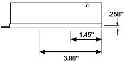
All dimensions are from the rear of the drive. They are to the center of the
hole. Be careful when drilling! These placements DO NOT line up with the
reinforced segments of the drive case. Be careful when tapping! Use a plug tap,
a normal tap would bottom out on the PCB.
The mounting holes do NOT line up with ANY holes on modern drives, even the
0661 drive holes WILL NOT FIT. The drive will mount upside down, there is no
other way to do it.
Additional features of the system unit include:
- One general purpose 32-bit full-length Micro Channel slot*
- Half-length Micro Channel slot
- 85-watt automatic voltage-sensing power supply
- Time and date clock with battery backup
- Integrated 16-grayscale plasma display, integrated version of IBM Enhanced
PC Keyboard.
* Some half-length cards that fit in a half-length slot may not fit in a
full-length slot.
Auto 16/4 Token Ring Fits Lower Slot
> the Auto 16/4 Token Ring fits into the bottom 16 bit
slot, almost like it was built for it.
Peter has a flashback and says:
The short 4Mbit on which the later 16/4 short design is based on
*was* in fact particularly designed for the P70 ... some time back in the late
80s when the P70 (and the P75) appeared in IBMs list there was a "short Token
Ring card" offered along with it, while the "normal PS/2" still got the
"toilet-seat 4 Mbit TR card".
The Token-Ring Network Model P70 386 Adapter/A (#1598) permits attachment of
the Model P70 386 (8573-061 and 8573-121) to the IBM Token-Ring Network. This
adapter is half-length and designed to fit in the short slot. It transmits and
receives at four million bits per second. To facilitate attachment to the IBM
Personal System/2 P70 386, a unique L angle connector with a permanently
attached short cable is provided.
8573-031 30 MB Hard Disk, 16 MHz planar
8573-061 60 MB Hard Disk, 20 MHz planar
8573-121 120 MB Hard Disk, 20 MHz
113 Error
This error code indicates a DMA timeout caused by a MCA card... if there is
nothing installed except the harddisk - replace that. It doesn't look like one,
but the 72-pin card-edge connector is in fact a MCA connector (Slot 4 in the
setup).
> As noted in a different thread: some series of 120 and 160MB HDs did
not run properly when installed "upside down" in the P70. Either they come up
with a 10482 error right after start -or- fail to LLFormat / run at all later
but operate fine otherwise when turned "upside up" again. (WD-3158,
WD-3160).
>> The -031 models used the infamous "energy conserving" harddisk,
which reduced spindle speed when in idle and spins up again when accessed. A
nerve killer!
> Like the Model 50Z and 70 the P70 had fairly lot of problems with
non-functional HDs. In the P70 *only* the black IBM WD-series drives had been
used for the 60 and 120MB models - like the WD-3158 120MB drive from the Model
70-121 / -A21.
Fitting a SCSI hard drive
From Bob Eager:
The P70 comes with one of the IBM
DBA-ESDI hard drives; these are the black ones that have a single wide edge
connector which is essentially the MCA bus; the controller is integrated on the
actual drive. These are not compatible with anything else, so the opportunity
for upgrading them is very limited.
One solution is to fit a SCSI disk, at the expense of one of the two slots
in the machine. This is what needs to be done:
- Open the case, and remove the disk cage (three screws, one on the bottom
and three inside). Also remove the disk cable from the planar.
- Fit a SCSI controller card. I used a standard IBM SCSI controller, with the
onboard terminator. It would be better to use one of the later ones with
automatic termination, if you have one, to save using an external terminator or
opening the case every time you want to plug in (say) a CDROM drive.
- Remove the old disk from the disk cage, and fit the new one. The disk I
used was a slim 350MB one; I had to drill some extra mounting holes to secure
it, and for safety I fitted a thin sheet of insulating material next to the
electronics board (I used part of an old CDROM sleeve).
- Get, or make, a SCSI cable. This is a 50 way cable with a 50 pin header on
one end, and a 50 pin edge connector on the other. I made a custom cable so
that it could be exactly the right length with no extra folds; there isn't much
room inside the P70 case.
- Install a power cable. This is the most fiddly bit. Obtain a standard 4 pin
drive power cable, with a few inches of wire on it. Choose one where the wire
isn't too thick, again to save space. Graft this into the output cables from
the power supply; I did this using automobile crimp connectors for joining two
wires together (just use a pair of pliers to close them).
- Fit the power cable to the drive, also the SCSI cable. Install the drive.
Finish by connecting the other end of the SCSI cable to the controller.
- Boot from the reference disk and run auto-configuration. Run diagnostic
tests, and with luck that will be it!
Early P70s Fail to Retain Configuration after Quick "On-Off-On"
>> DASDDRVR.SYS under DOS. Early P70 (16MHz version) tend to "spit
out" the configuration when you quickly power them off and back on.
>Not only the 16 MHz ones. I had this phenomenon on my 20 MHz Rev.1
(which is up and running again) also. Seems a common phenomenon for the first
PS/2 - which lacked a delay in the power supply. But the early 16MHz and all
Mod. 60 were pretty critical. If you didn't wait at least 20 seconds after a
power down you could have wrecked the config already.
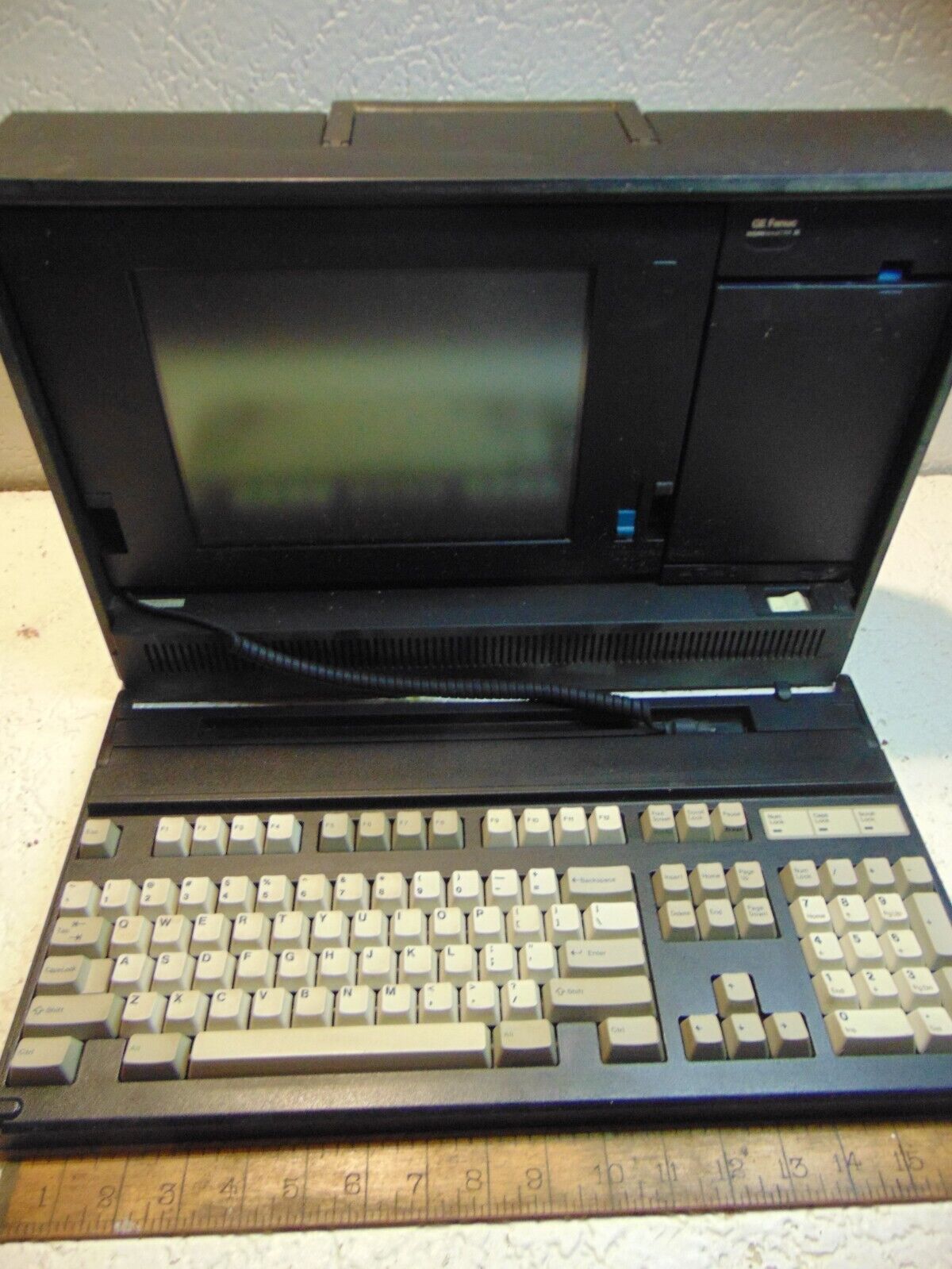
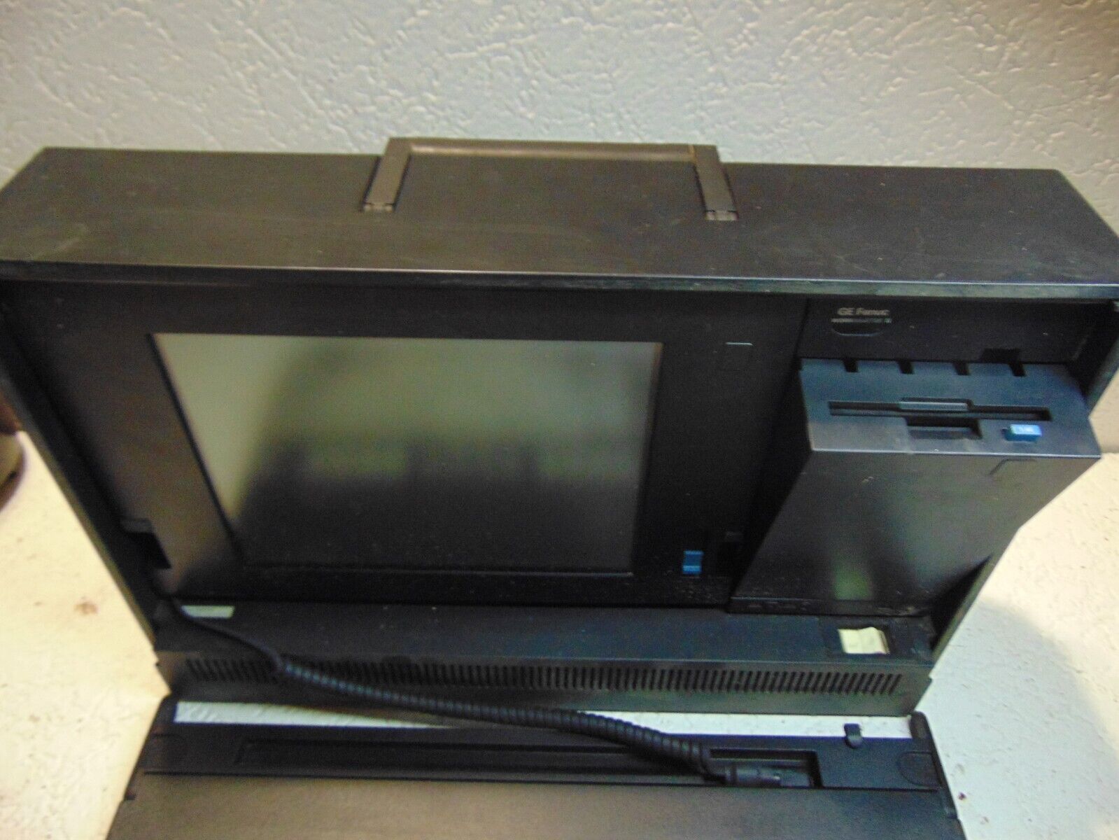
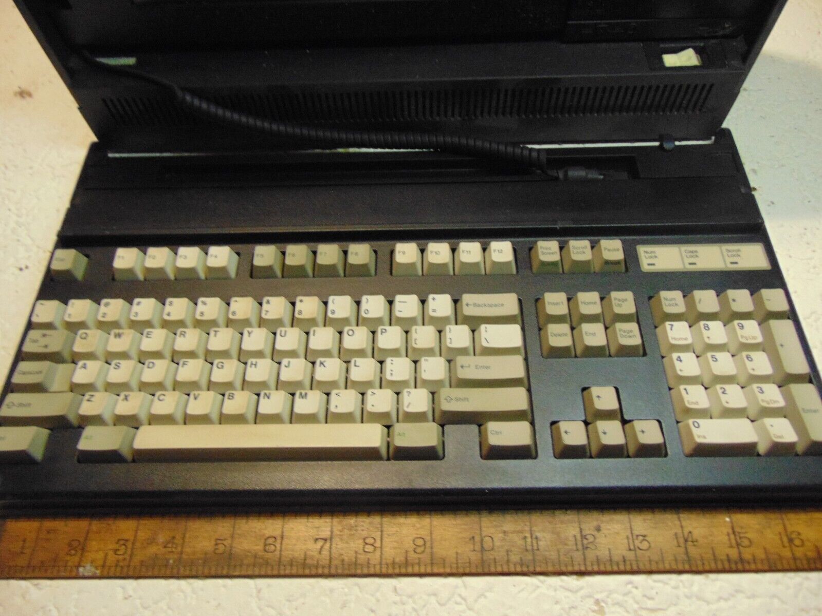
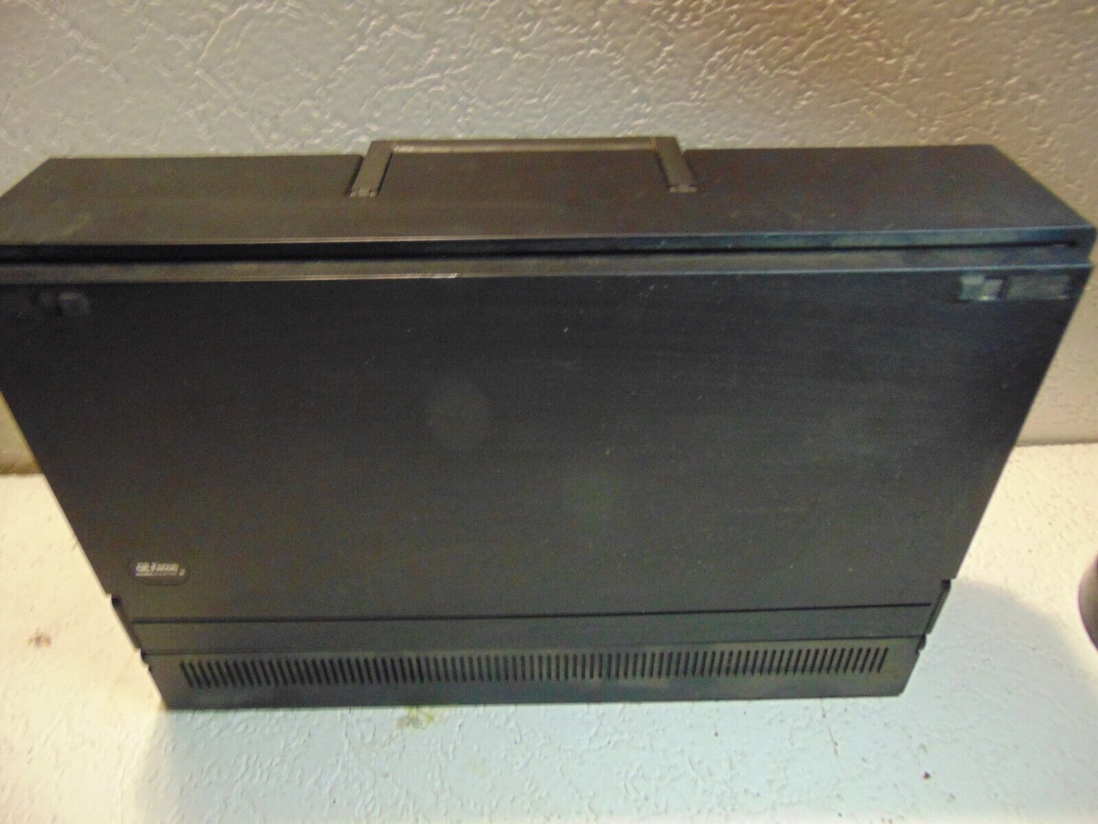
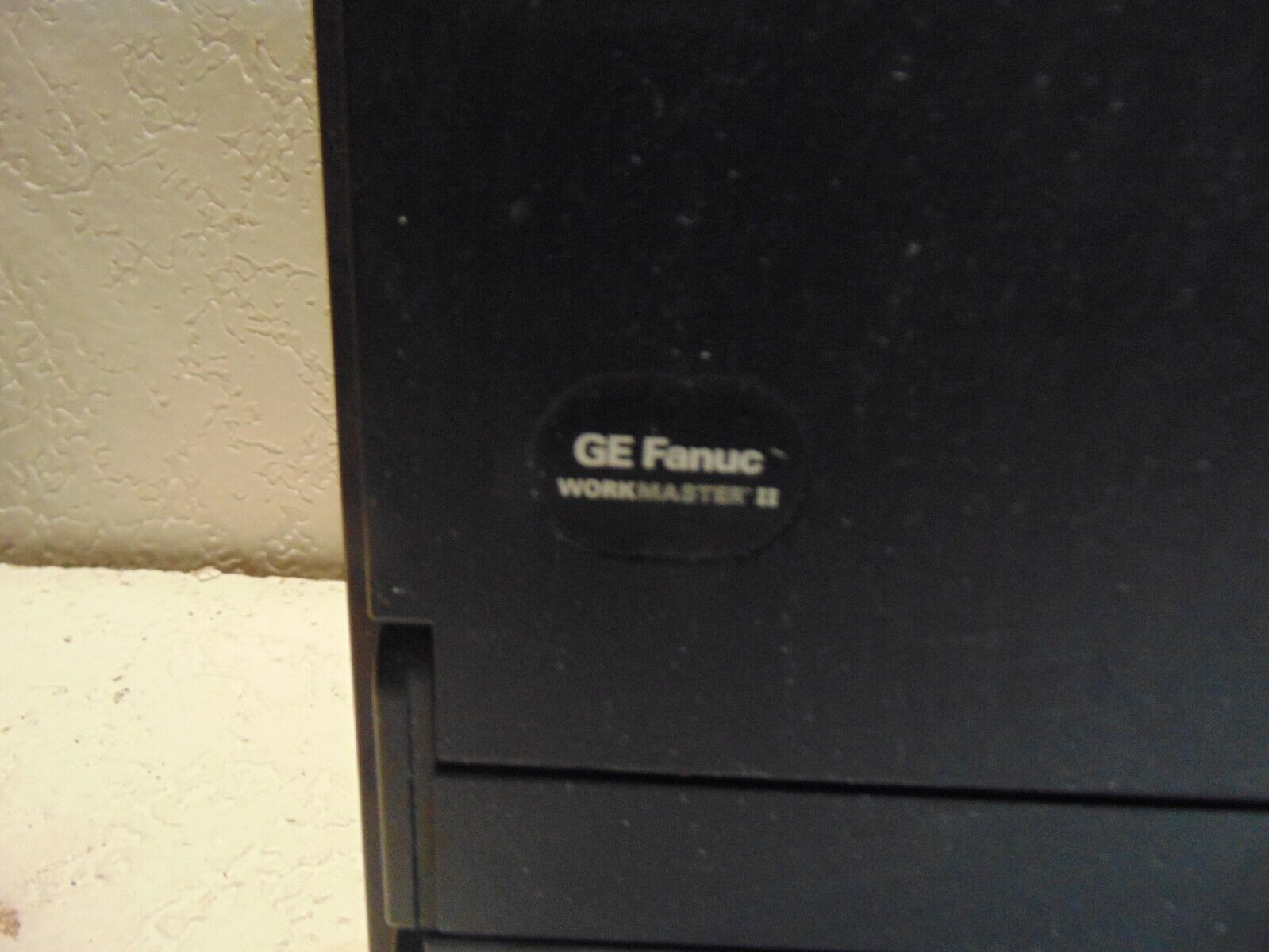
IBM 7186 - GE Fanuc Workmaster II
The IBM 7186 is a P70 in a black enclosure - officially named "GE Fanuc
Workmaster II"
It was sold for use with General Electric FANUC factory automation and
robotics equipment.
|
|
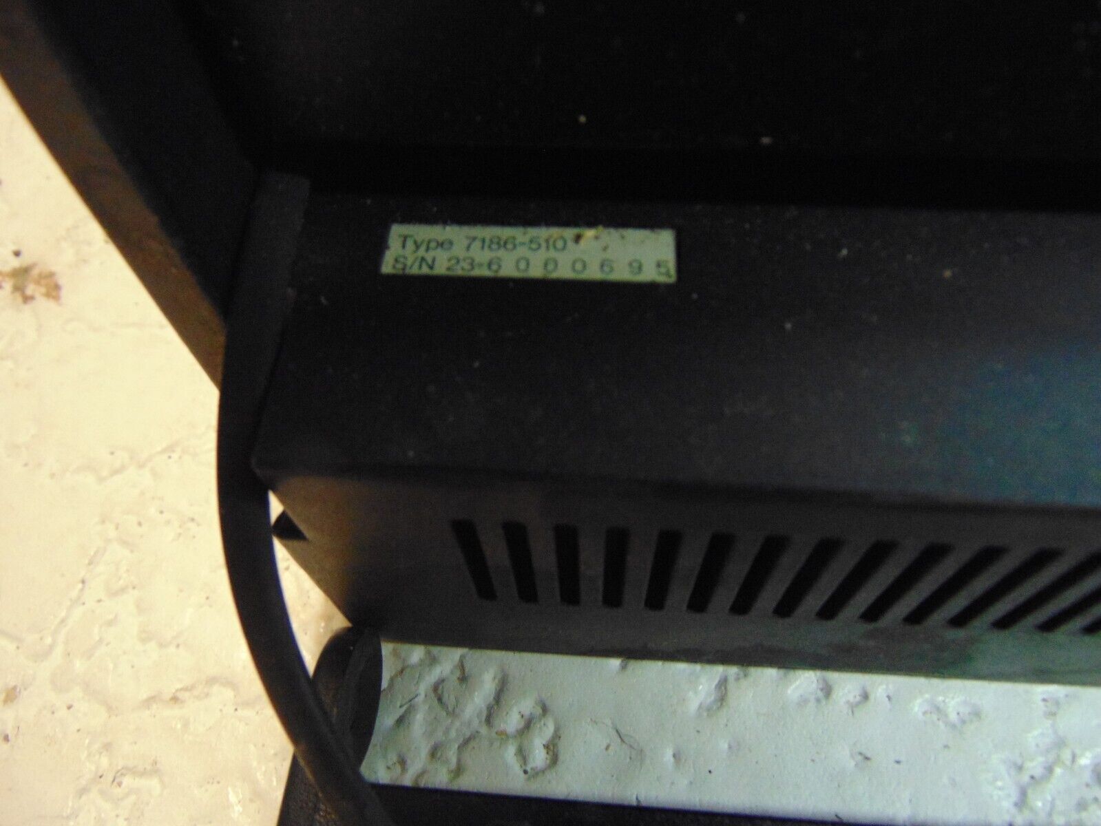
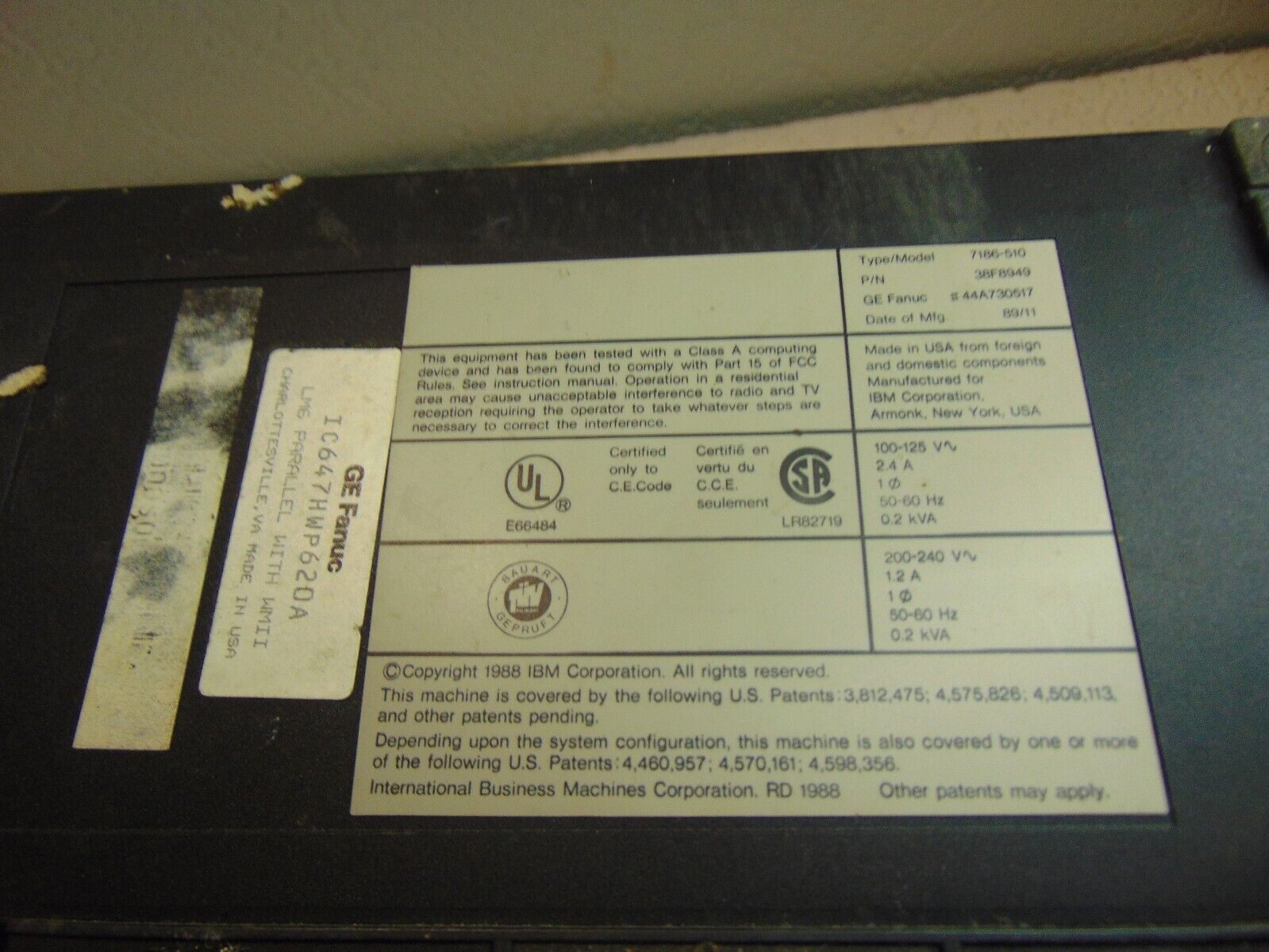
Type: 7186 (7186-510)
IBM P/N: 38F8949
GE Fanuc #: 44A730517
THEtechknight's sample uses the old P70 planar with
a 386DX CPU clocked at 16 MHz.
BIOS ROM: 38F5957 / 38F5958 (vanilla "old" 16 MHz P70)
|
Photos from ebay seller "oldphotos".
Videos:
Let's check out and fix a GE Fanuc Workmaster II 386 by THEtechknight
IBM PS/2 Portables Part 1 by uxwbill
|