|
Source: Parallel I/O ports for the IBM Micro Channel (original)
Authors: C. D. Spencer and E. J. Herrmann
Department of Physics, Ithaca College, Ithaca, New York 14850
Eight-bit parallel input/output (I/O) ports for the IBM Micro Channel are
described. First, the Micro Channel signals needed for the ports are identified
and defined. Next, the states of the data and address lines and the controls
during input and output sequences are described. Finally, ports circuitry which
responds to the sequences is presented and explained.
Introduction
Since the late 1970s, the vast majority of computer data acquisition papers
in the American Journal of Physics, The Physics Teacher, and recently this
journal involve interfaces and other circuitry designed by the authors. This is
not surprising since electronics and instrumentation are important in
physics.
Earlier, we characterized and compared game port, serial, and parallel
interfaces, and argued the advantages of the latter 1. We have also
described a comprehensive scheme for computer data acquisition through parallel
I/O ports 2. Others have presented a variety of instruments and
measurements which work off such ports (for instance, Refs. 3-7). Port designs
for Apple II's, 8,9 original PC's, 9 and Macintoshes
10 are in the literature. The purpose of this paper is to present
ports for the IBM Micro Channel.
I. I/O On Intel Microprocessors
Intel microprocessors perform input and output through timing sequences
(called machine cycles) which involve their data and address lines and several
control signals. In a programming language such as QuickBASIC, the output
sequence is produced by execution of an OUT port number, value statement. The
input sequence occurs when variable = INP(port number) is executed. Parallel
port circuitry must respond to the output sequence by storing the value (on the
data lines) and making it available to whatever is connected to the ports. The
circuitry must respond to the input sequence by supplying a value to the data
lines which is subsequently assigned to variable. In both cases, the circuitry
only acts when its "wired in" port number matches the port number in the
language statement.
II. Micro Channel Operations
The Micro Channel may be thought of as a set of sockets into which circuit
boards may be plugged. In the most common case, the sockets have three
sections: optional video extension, 8 bit, and 16 bit, as shown in Fig. 1. The
28 connections needed for the parallel ports are
A15...A0: 16 address lines contain the port number
during I/O operations; M/-IO: the memory or input/output control is low during I/O cycles and
high during memory read/write cycles; d7...d0: eight data lines on which values go to
and from the ports; -S1 & -S0: 2 status controls which distinguish
input from output cycles (-S0 and –S1, are 1 and 0 during inputs and 0 and 1
during outputs); -CMD: CoMmanD is the basic timing control.
Note that IBM uses the convention that signal names with "-" prefixes
are active low.
Figure 2 gives the timing for I/O sequences." Before -CMD goes active, two
things occur: (1) at least 85 ns before CMD, the port number appears on
A15...A0, and M/-IO indicates an I/O operation; and (2)
at least 55 ns before -CMD, S0 and S1, indicate an input
or output cycle.
Then, if the operation is an input, IBM specifies that the ports circuit
must put a data value on d7...d0 do no more than 60 ns
after -CMD (goes active) and it must be removed between 0 and 40 ns after
-CMD.
If the operation is an output, d7...d0 contains the
data value starting when -CMD goes active and continuing at least 30 ns after
-CMD returns inactive.
In the timing diagram: (1) "hatched" areas indicate unpredictable
states; (2) double lines on A15...A0 and
d7...d0 indicate a set of values, some high and some low;
and (3) the half-height lines for d7...d0 indicate a Hi-Z
"disconnected" state. Note that A15...A0, M/-IO,
S0, and S1, begin the next cycle during -CMD. Although
not shown, -CMD and the data lines may be finishing a previous cycle as the
cycle shown begins.
III. Ports Circuit
We decided to implement two 8-bit input and two 8-bit ports. Perusal of IBM
port number assignments for PS/2 Models 50, 60, 70, and 80 11
reveals that numbers 300 and 301 hex are not used by other devices such as the
keyboard, disk controller, printer ports, etc. (However, one must always be
sure no other board in a Micro Channel slot uses one of the numbers.)

Fig. 1. Pin assignments for a Micro Channel slot showing the
connections needed for parallel I/O ports.
The complete ports circuit in Fig. 3 contains three parts: 74F373 buffers, a
port number decoder, and a control generator. Each is discussed separately.
A. 74F373 Latch/Buffers
The heart of the ports are four 74F373 8-bit tri-state latch/buffers (on the
right in the figure). The OUT 300 and OUT 301 buffers store and continually
make available the last values output to 300 and 301 hex. The IN 300 and IN 301
buffers, upon execution of inputs from 300 and 301 hex, make available to the
Micro Channel the 8-bit value supplied to their data inputs.
The buffers require four controls:
When E300 (or E301) goes from high-to-low, the OUT300 (or OUT301) buffer
stores the value on the Micro Channel's d7...d0; activation of -OC300 (or -OC301) causes the IN 300 (or IN 301) buffer to
put the value at its data input on d7...d0.
The issue is how to generate the controls so that their actions occur at the
right point in the input and output sequences.
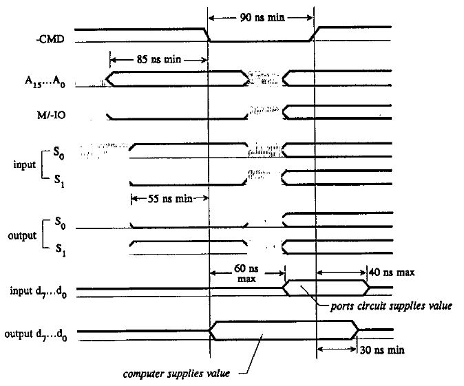
Fig. 2. Timing diagram for Micro Channel input and output
operations
B. Port Number Decoder
The circuit, containing 15 two-input OR gates and two inverters, responds to
the following binary values:
| A15...A1 |
A0 |
Port |
| 0000 0011 0000 000 |
0 |
0300 hex |
| 0000 0011 0000 000 |
1 |
0301 hex |
The signal -PND (port number decode) is active only when
A15...A0 corresponds to either 300 or 301 hex and when
M/-IO is low. (A0 is used in the control generator to distinguish 300 from
301.)
C. Control Generator
As stated earlier, A0, S0, S1, and the
signals which produce -PND start their next machine cycle before the end of
-CMD. Therefore, it is necessary to temporarily save A0,
S0, S1, and -PND. The 7475 latch does this (and the
values are held until the next -CMD).
The four 74F373 controls are produced by a 74F138 decoder IC. One of its
outputs, - Yi, is active only while –G2A and
–G2B are active (-PND is active) and while G1 is high
(during -CMD activation); i equals the binary value of CBA which equals
the saved value of S1S0A0. The four cases of
interest are:
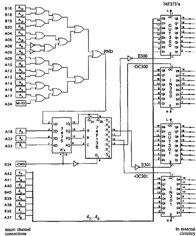
Fig. 3. Circuit for a pair of 8-bit input/output ports for
the Micro Channel.
| S1 |
S0 |
A0 |
i |
Case |
| 1 |
0 |
0 |
4 |
-Y4 after inversion is E300 |
| 0 |
1 |
0 |
2 |
-Y2 is -OC300 |
| 1 |
0 |
1 |
5 |
-Y5 after inversion E301 |
| 0 |
1 |
1 |
3 |
–Y3 is-OC301 |
The final issue is whether or not the controls occur at the right point in
the sequences. The three critical times are:
The port number decoder gate delays must be less than the 85 ns between
A15...A0, M/-IO, and -CMD. Using 74F IC's, the maximum
net delay is 35 ns. 12 In an input sequence, -OC300 (or -OC301) must place data on
d7...d0 no more than 60 ns after -CMD. Using
specifications for the inverter (for -CMD), the 74F138 and the 74F373, the
maximum gate delay is 27 ns. 12 In an output sequence, E300 (or E301) must go high-to-low within 30 ns
after -CMD while data is still on d7...d0. Using gate delay specifications for
the inverter (for -CMD), the 74F138, another inverter, and the 74F373, the
action occurs a maximum of 20 ns after -CMD. 12
IV. Construction and Testing
The ports circuit can be constructed on a Micro Channel wire wrap card for
$60. We put a 34-pin wire wrap edge socket on the card and use a ribbon cable
to carry the 4*8 = 32 port signals plus ground out of the computer. Power for
the circuit comes from Micro Channel connection A7 = +5V.
The I/O ports can be tested as follows:
- run the ribbon cable to a breadboard;
- enter and execute a program which outputs 0 to port 300 hex;
- check all bits with a logic probe;
- repeat for output values 1, 2, 4, 8, 16, 32, 64, and 128 and for output to port 301 hex;
- enter a program which inputs from 300 hex and prints the value;
- wire bit 0 low and run program [input 254 (1111 1110) since 74F373's "see" disconnected inputs as high];
- repeat for the other bits and for input from 301 hex.
V. Comments
Port numbers 300 and 301 hex were somewhat arbitrarily selected. Other
numbers could be used by changing the decoder circuit. Also, more than two
8-bit I/O ports are possible by leaving A1 (and perhaps
A2 and A3) out of the decoder, adding one or more
74F138's, and using the A's to select which 74F138 responds to the I/O
cycles.
All PS/2 machines support 16-bit I/O and higher models support 32-bit
operations. However, most popular languages presently available only do 8-bit
I/O (QuickBASIC, TurboPascal, etc.). However, if the language does 16-bit I/O,
a pair of 16-bit ports can be constructed by adding four 74F373's for data
bits d8...d15. (Pin assignments are: d8 = B48,
d9 = B48, d10 = A49, d11 = A50, d12
= B51, d13 = A51, d14 = B52, and d15 = B53.)
Also, the –CD DS16 control (A55) must be supplied to the Micro Channel. The
signal -PND meets timing specifications. However, errors will occur if 8-bit
I/O is done but the ports circuit signals via -CD DS 16 that it is a 16-bit
device.
The IBM [technical reference] states 11 that Micro Channel boards
must respond to a positive port number decode by activating the signal -CD
SFDBK (pin B36). We found this unnecessary. However, -PND meets specifications
for -CD SFDBK. The ports circuit was tested with QuickBASIC on a PS/2 Model 50
running DOS 4.0. For this situation, no special software or board response to
the "setup" cycle is needed. We do not know if this is the case under OS/2.
However, a programming language which executes machine code for 8- or 16- or
32-bit I/O to a port number should work independent of the operating
system.
Acknowledgment
The design, construction, and testing of the ports was supported by the
Clinton Ford Science Research Fund of Ithaca College.
References
- C. D. Spencer, P. Seligmann, and D. A. Briotta, Comput. Phys. 1, 59 (1987).
- C. D. Spencer, Digital Design for Computer Data Acquisition (Cambridge U.P., Cambridge, 1990), Chaps. 4-10.
- D. A. Briotta, P. F. Seligmann, P. A. Smith, and C. D. Spencer, Am. J. Phys. 55 (10), 891 (1987).
- A. Morales-Acevedo. E. Herrera, and H. Valencia, Comput. Phys. 3, 46 (1989).
- J. N. Dahiya and R. W. Freeman, Comput. Phys. 3, 49 (1989).
- G. P. Lietz, Am. J. Phys. 55(9), 796 (1987).
- J. Priest and J. Snider, Phys. Tech. 25(S), 303 (1987).
- J. A. Titus, D. G. Larsen, and C. A. Titus, Apple Interfacing (Blacksburg Group, Blacksburg, VA, 1981), Chaps. 1-3.
- C. D. Spencer, Digital Design for Computer Data Acquisition (Cambridge U.P., Cambridge, 1990). Chap. 3.
- R. E. Zammit and B. Taheri, Comput. Phys. 3, 77 (1989).
- IBM Personal System/2 Hardware Interface and Technical Reference (IBM, Poughkeepsie, NY, 1988)
- Fast Data Book (Fairchild Camera and Instrument Corp., So. Portland, ME, 1984), pp. 4-5, 4-14, 4-48, 4-231.
|