|
Based on Chet Heath's "Requirements for Advanced Bus Architecture"
Personal Systems Magazine, Issue 4 (physical page 7)
As with many things, IBM initially thought about extending and enhancing
the AT bus. They concluded that the AT bus, when limited to a single task
driving one peripheral, was sufficient. But that was totally altered when using
a multitasking system...
AT Electromagnetic Compatibility
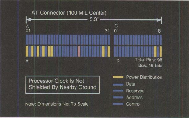
Let's unfold a card to visualize the EMC design problems of AT cards and the
systems that they support. Looking specifically at both sides of the connector
interface at once, and highlighting the radio frequency ground signals, one can
see that most of the signals do not have the close proximity of a radio
frequency shield. In fact, the processor clock was placed midway between two
radio frequency grounds. This was acceptable when the card format was designed
in 1978 for the 5140 machine, from which the PC was derived. That system had a
slow clock by today's standards.
Today, however, clock rates are much faster, data transfers are much faster,
and I/O devices move much more data in a shorter time. The result is
electromagnetic incompatibility with other nearby equipment and internal
interference between elements within the system cabinet. The security of the
data moving through the machine can even be compromised by others.
To prolong the life of the PC bus and allow extension to the 16-bit AT
interface, IBM introduced "single-point ground" power systems, conductive
plating of the power supply, frames and covers, and internal ground planes in
PC XT and later machines. But those measures become much more costly and less
effective as the speed of the systems increase. To understand why, let's go
back to basic electricity.
Many of us, in our youth, built electromagnets by winding turns of wire
around an iron nail or spike. We found that as we increased the area inside of
loops by creating more turns or accumulating area, the magnetism increased.
Also, when we increased the current by adding more batteries, we increased the
magnetism.
This is true for a fixed distance from the radiating element. The
electrostatic portion of the radio wave is proportional to the area inside of a
loop times the current that flows through that loop, and if it is an
alternating current or radio frequency, times the square of that frequency.
The data transitions on the computer bus are currents that alternate at very
high frequencies and thus have the potential to transmit energy (or receive
energy) as interference with other equipment either inside or outside the
box.
AT Radiated Electromagnetic Field
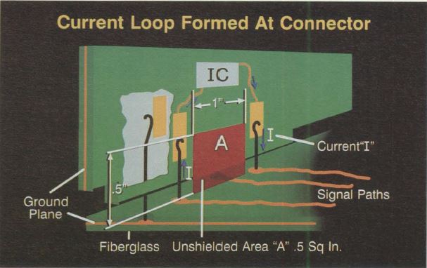
Look at the card connector in three dimensions. An unshielded area is formed
where the current flows on spring tabs to a card, through the card, and then
returns over spring tabs back to the system. Everywhere else in the system - on
the cards and on the system board - there is ground shielding, except at this
one point.
Using a radio frequency quiet room, IBM engineers found that the card
connector on the system board was the principal source of radiation from the
I/O bus when the interface between I/O and the system was active. This
unshielded area was considerably larger in the PC, PC XT and AT implementations
- about one-half square inch. In all of these systems, the ground system on the
cards is connected to the ground system or shield on the outside of the
case.
AT Card Grounding Mechanism
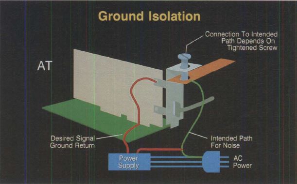
However, this meant that when the limited number of grounds in the AT was
inadequate to sink a current back to the power supply - for example, if the
card bracket retaining screw was not tightened firmly - the currents could flow
back through the metal system frame, which is the intended path for containing
noise in the PC, PC XT, or AT system.
If the mounting bracket is not electrically isolated, then there are only
the 3 pins on the PC Bus, which were intended only to provide a logic
reference, to ground the static. If the mounting screw is not tight, static may
go to ground through the card circuitry, possibly causing data alteration.
Also, the mounting screw does not guarantee that the card is actually centered
in the slot.
Current returning to the power supply could actually flow out over the
shields of cables and back through the AC power mains, forming a gigantic loop
called a "ground loop." Even with a small current flowing, this would create a
large loop area and very large radio signal. This is called "conducted
electromagnetic interference."
The ground mechanism used in the PC, PC XT, and AT also makes the system
susceptible to noise from outside the system. Energy from equipment connected
to the system could be coupled through the shield system. If the retaining
screw was not tightened, the current could sink through the card and through
the system rather than safely returning to the AC mains. Typically, this would
manifest itself as a data error when static discharges, perhaps from someone
touching adjacent equipment in a low-humidity environment. This data error
would not necessarily occur in the equipment that the person touched. In
extreme cases, a lightning strike could actually destroy local area network
(LAN) cards or communications cards where the screw is not tightened.
The design of the PC/AT bus is quite simple, with only three ground lines in
either design. On the motherboard, the shielding is adequate, but once the
signals rise up into the adapters, the shielding is much less and the signals
radiate more. Testing puts the limit to the PC/AT bus around 30-34 MHz due to
generated interference.
Smaller Footprint for Desktop
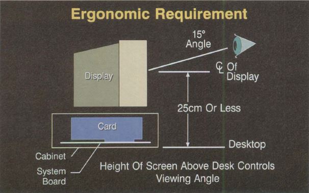
The smaller card can yield a smaller system, and also can assist in the
usability of the system. In several countries, industry regulations and public
laws define certain ergonomic characteristics of data entry terminals and
personal systems. One part of these requirements is the placement of the
centerline of the display no more than 25 centimeters above the desktop to
reduce glare and neck-muscle fatigue. With the common practice of pancake-like
stacking of the display and system unit to conserve desk space, the designer
has a choice of a smaller screen or a smaller card.
Micro Channel cards are 3.5 inches high, the same height as the connectors
to peripherals on the rear bracket of PC, PC XT, and AT cards. PS/2 systems,
therefore, maintain connection to most AT peripherals while permitting larger
size displays to be installed where ergonomics is a consideration.
However, Micro Channel architecture does not restrict the card height to 3.5
inches. While this is a specification for existing PS/2 computers, systems with
capability for larger cards are feasible.
AT vs MCA Card Size Comparison
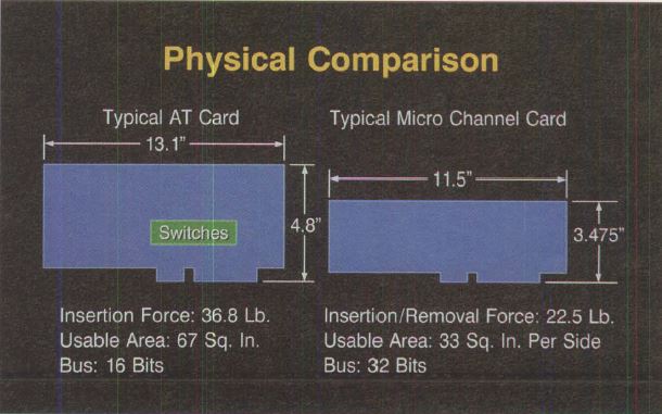
Look at a physical comparison of an AT card and a Micro Channel card. On
initial inspection, the Micro Channel card is physically smaller. This allows
for a smaller system. However, the card format is optimized for surface-mount
technology (SMT). The connector dimensions match the tab spacing on SMT
components, facilitating wiring of the card.
SMT allows an increase in the vertical and horizontal densities, each by a
factor of 2-to-1, for an overall aerial density improvement of 4-to- l. Surface
mounting also allows the implementation of components on both sides of the
board for a total improvement of 8-to- l in component density.
MCA Edgecard Alignment
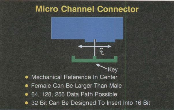
The Micro Channel connector uniquely references mechanical alignment from a
keyway centered in the connector, allowing tighter control of mechanical
tolerances. When inserted in a 32-bit socket, neither end of a 16-bit male
connector is in contact with the end of the female socket. Likewise, a 16- or
32-bit card could be inserted into a 64-bit or larger socket and align
perfectly. A 32-bit card has been designed that leaves clearance at the end
bulkhead position for a 16-bit connector. Therefore, this 32-bit design can be
used in 16- or 32-bit or larger systems. A single design can be made for all
systems and still be capable of 32-bit throughput.
MCA Static Grounding
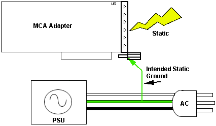
The MCA grounding and mounting scheme eliminates the problems of the ISA
bracket. The MCA slot bracket has several spring fingers to maintain positive
contact with the sides of the slot. The metal bracket blocks radiation that
would otherwise leak from the slot. It is electrically isolated from the card
circuitry, thus reducing the possibility of data alteration.
Instead of depending on a mounting screw at the top, the mounting bracket
actually fits inside of a frame that is at the rear of the system, and this
provides positive centering of the adapter. In addition, the V-shaped slot at
the bottom of the MCA slot bracket fits around a knurled thumbscrew, ensuring a
tight fit.
AT vs. MCA Pin Spacing
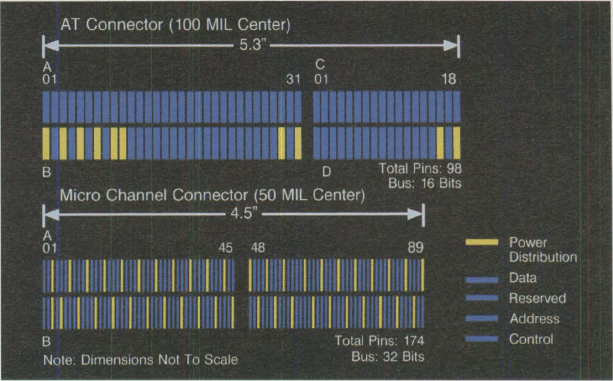
The spacings on the connector have been cut to one-half of the spacings used
on the AT connector. A Micro Channel 16-bit socket is approximately the same
size as a PC 8-bit socket. The Micro Channel 32-bit connector is actually
smaller than the AT 16-bit connector. This follows the trend of other
components in the system, such as processors that have grown in power from the
8-bit interface of the 8088 processor to the 16-bit 80286 and the 32-bit 80386
without growing significantly in physical size.
The number of signals in the connector has been doubled, and the insertion
and removal forces have been cut almost in half. This is extremely important
because in manufacturing and service situations, had the length of the
connector increased or more tabs been defined, either the insertion force or
removal force would have exceeded 40 pounds.
We have designed out the electromagnetic compatibility problems of the AT
connector. One can see by the pattern in the lower half that each signal in the
Micro Channel bus is situated between a ground, across from a ground, or
adjacent to a ground signal. There is a radio frequency shield on every fourth
pin. On the opposite side of the connector, the pattern is identical but offset
by two pin spacings. The area between the closest shield and a signal is
thereby diminished significantly.
MCA Radiated Electromagnetic Field Strength
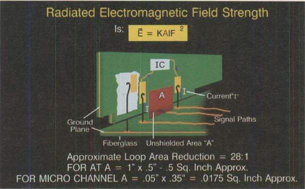
The loop area of the Micro Channel bus is one-twenty-eighth of that for the
AT bus. The signal transitions can then increase in frequency, by a factor of
the square root of 28, or approximately five times. This has been
experimentally verified outside of IBM - studies of the Micro Channel bus have
shown a cutoff frequency above 80 MHz. Studies of the AT bus have shown a
cut-off frequency of approximately 16 MHz, or again the same factor of
5-to-1.
|