|
Introduction
Physical Interface
Connector Pinouts
Connector 1 (Rear)
Connector 2 (Front)
Signal Descriptions
Micro Channel Signals
Memory Signals
Other Signals
Power
The pinout reverse engineered (328 pins, oof!) and drawings created by Tomáš Slavotínek.
Introduction
The Processor Complex interface
(also known as "Processor Interface Connection") consists of Micro Channel
signals (some of which are shared with the planar I/O bus), memory signals,
control signals, power supply lines, and some other connections.
A list of machines that use the Processor Complex interface can be found
HERE.
Physical Interface
The physical interface consists of two identical connectors. The connector
used is an unique variant of the Micro Channel connector with 2x40 + 2x42 pins
(82 usable positions = 164 usable pins; or 84 positions including the space
taken by the physical key). This gives a total of 328 usable pins for both
connectors. The connectors are placed in-line with no gap in between, touching
each other by the shorter 2x40-pin section (rotated by 180°).
Connector Type
Burndy Computerbus CEE2X82S-8Z14, CEE2X82SP-8Z14 (-V8Z14) or AMP 646215-1
Connector Pinouts
The "component side" (A) and "solder side" (B) refers to an installed processor card.
The "Rear" arrow points towards the back side of the planar/system unit.
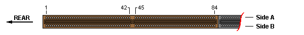
Connector 1 (Rear)
Micro Channel (and planar I/O) bus connections + some memory signals.
Some signals still unknown.
| Pin | Signal | | Pin | Signal |
|---|
| B01 | MA AB 0 | A01 | MA AB 1 |
| B02 | MA AB 2 | A02 | MA AB 3 |
| B03 | GND | A03 | MA AB 4 |
| B04 | MA AB 5 | A04 | MA AB 6 |
| B05 | MA AB 7 | A05 | +5 Vdc |
| B06 | MA AB 8 | A06 | MA AB 9 |
| B07 | -DPAREN | A07 | RAS A4 1/3 |
| B08 | DPAR(0) | A08 | RAS A4 0/2 |
| B09 | GND | A09 | RAS A3 1/3 |
| B10 | DPAR(1) | A10 | +5 Vdc |
| B11 | DPAR(2) | A11 | RAS A3 0/2 |
| B12 | Unknown (out) | A12 | -RESET |
| B13 | Unknown | A13 | Unknown |
| B14 | -CD DS 16 | A14 | CD CHRDY |
| B15 | GND | A15 | -CD DS 32 |
| B16 | 14.3 MHz OSC | A16 | GND |
| B17 | GND | A17 | -CD SFDBK |
| B18 | MADE 24 | A18 | A 23 |
| B19 | A 11 | A19 | A 22 |
| B20 | A 10 | A20 | A 21 |
| B21 | A 09 | A21 | +5 Vdc |
| B22 | GND | A22 | A 20 |
| B23 | A 08 | A23 | A 19 |
| B24 | A 07 | A24 | A 18 |
| B25 | A 06 | A25 | A 17 |
| B26 | GND | A26 | WE AB |
| B27 | A 05 | A27 | A 16 |
| B28 | A 04 | A28 | A 15 |
| B29 | A 03 | A29 | A 14 |
| B30 | GND | A30 | +5 Vdc |
| B31 | A 02 | A31 | A 13 |
| B32 | A 01 | A32 | A 12 |
| B33 | A 00 | A33 | -PREEMPT |
| B34 | GND | A34 | -BURST |
| B35 | -ADL | A35 | -CMD |
| B36 | -CHRDYRTN | A36 | GND |
| B37 | ARB 00 | A37 | ARB 01 |
| B38 | ARB 02 | A38 | ARB 03 |
| B39 | GND | A39 | ARB/-GNT |
| B40 | -TC | A40 | +5 Vdc |
| B41 | -S0 | A41 | -S1 |
| B42 | M/-IO | A42 | D 00 |
| B43 | PHYSICAL KEY | A43 | PHYSICAL KEY |
| B44 | PHYSICAL KEY | A44 | PHYSICAL KEY |
| B45 | D 01 | A45 | D 02 |
| B46 | D 03 | A46 | +5 Vdc |
| B47 | GND | A47 | D 04 |
| B48 | D 05 | A48 | D 06 |
| B49 | D 07 | A49 | D 08 |
| B50 | D 09 | A50 | GND |
| B51 | D 10 | A51 | D 11 |
| B52 | D 12 | A52 | D 13 |
| B53 | GND | A53 | D 14 |
| B54 | D 15 | A54 | -SDR(0) |
| B55 | -SDR(1) | A55 | -SD STROBE |
| B56 | -DS 16 RTN | A56 | +5 Vdc |
| B57 | -REFRESH | A57 | -SBHE |
| B58 | -CHCK | A58 | -MSDR |
| B59 | GND | A59 | DPAR(3) |
| B60 | D 16 | A60 | +5 Vdc |
| B61 | D 17 | A61 | D 18 |
| B62 | D 19 | A62 | D 20 |
| B63 | D 21 | A63 | D 22 |
| B64 | D 23 | A64 | GND |
| B65 | GND | A65 | D 24 |
| B66 | D 25 | A66 | D 26 |
| B67 | D 27 | A67 | D 28 |
| B68 | D 29 | A68 | +5 Vdc |
| B69 | D 30 | A69 | D 31 |
| B70 | A 24 | A70 | A 25 |
| B71 | GND | A71 | A 26 |
| B72 | A 27 | A72 | A 28 |
| B73 | A 29 | A73 | A 30 |
| B74 | A 31 | A74 | +5 Vdc |
| B75 | -BE 0 | A75 | -BE 1 |
| B76 | -BE 2 | A76 | -BE 3 |
| B77 | GND | A77 | TR 32 |
| B78 | WE BB | A78 | -DS 32 RTN |
| B79 | Unknown | A79 | -IRQ 05 |
| B80 | INTR | A80 | +5 Vdc |
| B81 | Unknown (in?) | A81 | -MMC |
| B82 | -MMC CMD | A82 | Unknown |
| B83 | GND | A83 | MA AA 0 |
| B84 | MA AA 1 | A84 | MA AA 2 |
Note: All "unknown" pins serve a purpose. There
are no unused positions.
(in/out) indicates the direction of the signal from the processor card's point
of view.
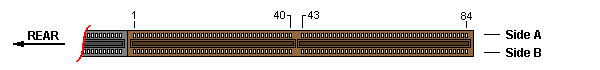
Connector 2 (Front)
Almost exclusively memory signals.
| Pin | Signal | | Pin | Signal |
|---|
| B01 | MA AA 3 | A01 | MA AA 4 |
| B02 | MA AA 5 | A02 | MA AA 6 |
| B03 | GND | A03 | MA AA 7 |
| B04 | MA AA 8 | A04 | MA AA 9 |
| B05 | MA BB 0 | A05 | GND |
| B06 | MA BB 1 | A06 | MA BB 2 |
| B07 | MA BB 3 | A07 | MA BB 4 |
| B08 | GND | A08 | MA BB 5 |
| B09 | MA BB 6 | A09 | MA BB 7 |
| B10 | MA BB 8 | A10 | +5 Vdc |
| B11 | MA BB 9 | A11 | MA BA 0 |
| B12 | MA BA 1 | A12 | MA BA 2 |
| B13 | GND | A13 | MA BA 3 |
| B14 | MA BA 4 | A14 | +5 Vdc |
| B15 | MA BA 5 | A15 | MA BA 6 |
| B16 | MA BA 7 | A16 | MA BA 8 |
| B17 | GND | A17 | MA BA 9 |
| B18 | MD A 0 | A18 | +5 Vdc |
| B19 | MD A 1 | A19 | MD A 2 |
| B20 | MD A 3 | A20 | MD A 4 |
| B21 | GND | A21 | MD A 5 |
| B22 | MD A 6 | A22 | MD A 7 |
| B23 | MD A 8 | A23 | MD A 9 |
| B24 | MD A 10 | A24 | GND |
| B25 | MD A 11 | A25 | MD A 12 |
| B26 | MD A 13 | A26 | MD A 14 |
| B27 | GND | A27 | MD A 15 |
| B28 | MD A 16 | A28 | MD A 17 |
| B29 | MD A 18 | A29 | MD A 19 |
| B30 | MD A 20 | A30 | +5 Vdc |
| B31 | MD A 21 | A31 | MD A 22 |
| B32 | MD A 23 | A32 | MD A 24 |
| B33 | GND | A33 | MD A 25 |
| B34 | MD A 26 | A34 | MD A 27 |
| B35 | MD A 28 | A35 | MD A 29 |
| B36 | MD A 30 | A36 | GND |
| B37 | MD A 31 | A37 | MDP A 0 |
| B38 | MDP A 1 | A38 | MDP A 2 |
| B39 | GND | A39 | MDP A 3 |
| B40 | BS A 0 | A40 | +5 Vdc |
| B41 | PHYSICAL KEY | A41 | PHYSICAL KEY |
| B42 | PHYSICAL KEY | A42 | PHYSICAL KEY |
| B43 | BS A 1 | A43 | BS A 2 |
| B44 | BS A 3 / MA A 11 * | A44 | WE AA |
| B45 | WE BA | A45 | RAS A1 0/2 |
| B46 | RAS A1 1/3 | A46 | +5 Vdc |
| B47 | GND | A47 | RAS B1 0/2 |
| B48 | RAS B1 1/3 | A48 | RAS A2 0/2 |
| B49 | RAS A2 1/3 | A49 | RAS B2 0/2 |
| B50 | RAS B2 1/3 | A50 | GND |
| B51 | CAS A 0 | A51 | CAS A 1 |
| B52 | CAS A 2 | A52 | CAS A 3 |
| B53 | GND | A53 | CAS B 0 |
| B54 | CAS B 1 | A54 | CAS B 2 |
| B55 | CAS B 3 | A55 | -CASP A / MA A 10 * |
| B56 | -CASP B / MA B 10 * | A56 | +5 Vdc |
| B57 | MD B 0 | A57 | MD B 1 |
| B58 | MD B 2 | A58 | MD B 3 |
| B59 | GND | A59 | MD B 4 |
| B60 | MD B 5 | A60 | +5 Vdc |
| B61 | MD B 6 | A61 | MD B 7 |
| B62 | MD B 8 | A62 | MD B 9 |
| B63 | MD B 10 | A63 | MD B 11 |
| B64 | MD B 12 | A64 | GND |
| B65 | GND | A65 | MD B 13 |
| B66 | MD B 14 | A66 | MD B 15 |
| B67 | MD B 16 | A67 | MD B 17 |
| B68 | MD B 18 | A68 | +5 Vdc |
| B69 | MD B 19 | A69 | MD B 20 |
| B70 | MD B 21 | A70 | MD B 22 |
| B71 | GND | A71 | MD B 23 |
| B72 | MD B 24 | A72 | MD B 25 |
| B73 | MD B 26 | A73 | MD B 27 |
| B74 | MD B 28 | A74 | GND |
| B75 | MD B 29 | A75 | MD B 30 |
| B76 | MD B 31 | A76 | MDP B 0 |
| B77 | GND | A77 | MDP B 1 |
| B78 | MDP B 2 | A78 | MDP B 3 |
| B79 | BS B 0 | A79 | BS B 1 |
| B80 | BS B 2 | A80 | +5 Vdc |
| B81 | BS B 3 / MA B 11 * | A81 | ECC PD |
| B82 | RAS B3 0/2 | A82 | RAS B4 1/3 |
| B83 | GND | A83 | RAS B4 0/2 |
| B84 | MMCR RTN | A84 | RAS B3 1/3 |
Notes:
* The marked pins are multiplexed
on the Type 4 complex to realize support for 16 and 32 MB ECC memory
modules that require 11x11 or 12x10 addressing. SIMMs with a non-standard
pinout are required!
Signal Descriptions
The Processor Complex interface consists of:
Throughout this page, a minus sign (-) in front of a signal name indicates
that the signal is active when it is at a low-voltage level. When no minus sign
appears, the signal is active when it is at a high-voltage level. For example,
-CMD specifies the signal is active low. Also, ARB/-GNT is in the ARB state
when it is at a high level and is in the -GNT state when it is at a low
level.
All of the logic signal lines are transistor-transistor logic (TTL)
compatible.
Micro Channel Signals
32-bit Micro Channel interface. All Micro Channel Signals are
described HERE.
Note: Some of the channel data, address, and
control signals are shared with the planar I/O bus. This bus interconnects all
the on-planar features - external I/O ports, FDC, Op Panel interface, memory
Presence Detect lines, etc.
Memory Signals
Two 32-bit interfaces (64-bit total) between the memory controller on the
processor card and the memory SIMMs on the planar. The memory is organized as
two independent memory banks - Bank A and Bank B. Each bank then consists of
two SIMM pairs:
- Pair A - SIMM slots 1 and 2
- Pair B - SIMM slots 3 and 4
Some signals are unique to each SIMM slot, some are shared within the
individual SIMM pairs, and some are shared by the entire bank.
MA bp xx: Memory Address Bit xx for Bank b Pair p
MD b xx: Memory Data Bit xx for Bank b
MDP b x: Memory Data Parity Bit x for Bank b
BS b x: Block Select x for Bank b
WE bp: Write Enable for Bank b Pair p
CAS b x: Column Address Strobe x for Bank b
-CASP b: Column Address Strobe Parity for Bank b
RAS bs x/y: Row Address Strobe x and y for Bank b Slot s
ECC PD: Error-Correcting Code Presence Detect: This signal is driven
by the planar logic and it's the negative AND of -ECC PD from each SIMM
connector (pin 48). If any of the SIMM slots is occupied by a ECC memory
module, this signal is driven high. Low otherwise.
Other Signals
-RESET: -System Reset: This signal is driven by the planar logic.
INTR: Interrupt Request: This signal is driven by the planar
interrupt controller and is connected to the INTR pin of the main
processor.
MMCR RTN: Matched Memory Cycle Request Return: This signal is driven
by the planar logic and it's the AND of -MMCR from each channel connector.
Power
The only voltage available on the Processor Complex interface is +5 V DC.
Pins supplying this voltage are located on the A side of the connectors,
together with some ground pins. A majority of the ground pins is then located
on the B side.
Any other voltages are generated locally on the processor board, from the
+5 V DC supply rail.
|