|
Introduction
Systems with EEPROM
EEPROM Devices
Programming Interface (Pads)
External Programming
Further Reading
Disclaimer: Tinkering with the serial EEPROM and
its contents may render the entire planar unusable if the user is unable to
correct their actions! The author is in no way responsible for any damage
caused by the use of the presented information.
Content by Tomáš Slavotínek. Last update: 19 Nov 2023
Introduction
Most late PS/2 machines come with a small (1 kbit) EEPROM storage located on
the planar. The EEPROM is used to store the following information:
- Privileged-Access Password (PAP)
- Vital Product Data (VPD)
- Selectable Boot (IPL) sequence?
- possibly more
All EEPROM-equipped PS/2s use the 10G4672
I/O Controller to interface with the EEPROM. Later PC Series and PC Server
machines use a different control logic.
Limited access to the EEPROM's contents is provided via the Int 15h AH=D2h
BIOS interface.
Systems with EEPROM
PS/2 Line
PC and PC Server
EEPROM Devices
The following EEPROM devices can be found on various PS/2 and other IBM
planars:
Note: It's unknown whether the larger 2 kbit
EEPROM device is used to its full capacity or if it was selected for other
reasons (e.g. supply chain).
These so-called "Microwire" EEPROMs use an early iteration of what we
know today as the Serial Peripheral Interface (SPI). See the
"External Programming" section for information on
how to program these devices.
Programming Interface (Pads)
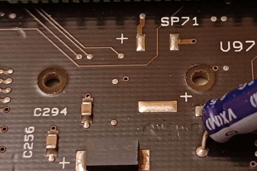
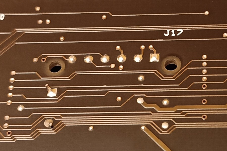
All EEPROM-equipped PS/2 planars have a programming interface on the solder
side of the PCB. It consists of six tinned pads with two adjacent holes. The
pads are likely intended to meet with a set of pogo pins/test needles. The
holes would be needed to hold the probe assembly in place and keep the pins
under pressure to achieve a reliable connection.
9585 "X" planar EEPROM prog. interface
Component side - retention holes |
9585 "X" planar EEPROM prog. interface
Solder side - row of contact pads (J17) |
Interface Pinout
| Pin | Signal Name | Description |
|---|
| 1 | EEPROM_CS, CS, S | Chip Select Input; EEPROM pin 1, 10G4672 pin 32 |
| 2 | SERIAL_CLK, SK, C | Serial Clock; EEPROM pin 2, 10G4672 pin 58 |
| 3 | SERIAL_DATA_IN, DI, D | Serial Data Input; EEPROM pin 3, 10G4672 pin 114 |
| 4 | SERIAL_DATA_OUT, DO, Q | Serial Data Output; EEPROM pin 4, 10G4672 pin 116 |
| 5 | GND, Vss | Ground; EEPROM pin 5; common ground |
| 6 | ? | Support logic high-Z input? 10G4672 pin 133 |
Notes:
- The signal names are taken from the various EEPROM datasheets and IBM TDB. See the EEPROM Devices section for links.
- The pin 1 pad is square-shaped, while all the other pads are round.
- Pin 6 - Possibly used to put the support logic (I/O controller) EEPROM interface to high-impedance mode so it doesn't interfere with the programming process. (Needs confirmation.)
The programming interface doesn't provide a means of powering the EEPROM
device. Therefore, the entire planar must be powered using the main PSU
connector during the programming process (at the very least, the 5 V supply
must be present).
External Programming
The interface together with some external equipment can be used to recover a
planar that has been bricked by setting the Privileged-Access Password (PAP).
Probably the easiest way of reading/writing/erasing these devices is to use
an EEPROM programmer with support for serial devices. Cheap USB programmers can
be bought online. Make sure it supports the 93Cxx EEPROM series. (search terms:
"BIOS programmer", "serial EEPROM programmer", "CH341", "CH341B", "CH341B",
etc.)
Further Reading
|