|
Introduction
Dual Bus Operation
Single Bus Operation
Enhanced Dual Path Memory
Source: PS/2 Models 95 XP 486, 90 XP 486, 55LS and P75 486 Fundamentals (pp 53, 57 & 58)
Introduction
When bus masters were implemented on Micro Channel servers, it was found
that there was often contention for memory access between the processor and the
bus masters, and that the processor was being delayed waiting for bus masters
to release the path into memory.
The new design of the processor complexes addresses these issues by
providing a Dual Path into memory (aka Dual Bus Memory),
effectively providing two paths to system memory, one from the processor and
one from the Micro Channel. These two separate paths to system memory allow
overlapping of processor and bus master cycles.
Note: Dual Path memory should not be confused with
Interleaved Memory.

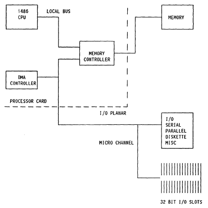
Figure 1. System Block Diagram of Dual Bus System
There are two paths to the memory through the memory controller:
- A path from the CPU
- A path from the Micro Channel
So, the CPU does not have a dedicated path to memory, instead, it can share
access to the memory with a Bus Master. If you think about it, having a
dedicated path would mean adding another 32 lines to the complex interface.
Why is this limited to the CPU and Bus Masters? If an adapter is being run
PIO, that means the CPU is a lot more involved with controlling that adapter. A
bus master can execute it's own operations.
Note: The memory used in the IBM PS/2 Model 90 and
95 XP 486 systems (and other models) is dual bus NOT
dual-ported so the CPU may be held off for the current bus master
transfer to complete, but not the full transfer.
Note: Type 2
complexes do not support Dual Path Memory.
Dual Bus Operation

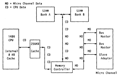
Figure 2. Dual Bus Operation
A bus from the CPU to the memory controller, and a bus from the Micro
Channel to the memory controller allows the CPU to use the system memory, while
at the same time a bus master can be using the Micro Channel. The net result of
this is a significant increase in processing power, but this will not be seen
if you are using single tasking software, or running only one task in a
multitasking environment.
In the Model 90 and 95 XP 486 systems the memory controller alternates
access to the system memory between the CPU and any bus master. This will
happen even if the bus master is controlling the bus to the memory. This can be
seen in Figure 2 in the interleaving of Micro Channel Data (MD) with CPU
Data (CD) between the memory controller and the memory.
During the time that a bus master has control of the system, the CPU can
access the system memory. If a transfer is in process at the same instant that
the CPU wants to use the memory, the CPU will be held off until that one part
of the transfer has finished. It does not have to wait for the total transfer
to have finished as in previous PS/2 systems. The wait for memory access is now
@ 300 - 500 ns compared with up to 7 microseconds in previous PS/2 systems.

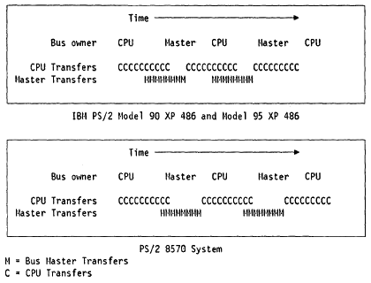
Figure 3. Dual Bus Timing
Figure 3 shows that the IBM PS/2 Model 90 and 95 XP 486 systems allow
CPU cycles to overlap bus master cycles more than in previous systems. The CPU
executes cycles even after a bus master starts executing cycles, but the PS/2
8570 hits a cycle that locks the CPU out much sooner than the IBM PS/2 Model 90
and 95 XP 486 systems.
Three kinds of overlapped cycles can occur:
CPU reads to L2 cache simultaneously with bus master I/O
When the microprocessor is reading from or writing to its internal
cache or to the optional 256 KB cache, the bus master that is controlling the
Micro Channel bus has exclusive access to system memory. CPU reads to L2 cache simultaneously with bus master memory access
The microprocessor and the bus master that is controlling the Micro
Channel bus can use the system memory at the same time, provided that they
do not try to use the same memory locations. CPU reads to memory simultaneously with bus master I/O
When a bus master is reading from or writing to an I/O device or
an adapter in a Micro Channel expansion slot, the microprocessor has exclusive
access to system memory.
In computers that do not have a dual bus, the microprocessor is the default
master, which means that it has to wait until no other masters are controlling
the Micro Channel bus before it can have access to system memory.
Single Bus Operation
Without a dual path bus, there is often contention for
system resources such as main memory. When contention between the processor
and a bus master occurs, one has to wait for the other to finish its memory
cycle before it can proceed. Thus, fast devices such as processors have
to wait for much slower I/O devices, slowing down the performance of the
entire system to the speed of the slowest device. This is very costly to
the overall system performance.

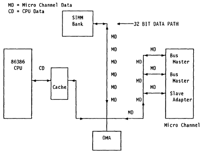
Figure 4. Single Bus Operation
The bus master can hold the system bus, and as there is only one bus, it
does not matter to which part of the system the bus master is transferring
data. The CPU will have to wait, and arbitrate for control of the system bus,
so that it can get to the system memory. This was good for the bus masters, but
not so good for the CPU. When a bus master took control of the system bus, the
processor had to wait for the bus master to release the bus, or had to
arbitrate for control of the bus. This could take up to 7 microseconds.
Enhanced Dual Path Memory
Although Type 1 and complexes allow both the
processor and busmasters to access memory concurrently through two paths, the
Type 3 and Type 4
has buffers at both paths to provide better performance. Also the buffer on the
adapter side (I/O buffer) uses packet data transfers for writes. This means 16
bytes are collected and this packet is written in one cycle to memory as
opposed to writing for every 4 bytes received (as with unbuffered systems).
|