|
194-031 IBM PS/2 486SLC3 Processor Upgrade (summary only)
IBM 486SLC3 Processor Upgrade FCC ID ANOIBM486SLC3

|
VR1 LT1085CT
U1 Reverse of mounting pins
U2 Socket for PLCC 387SX
U4 486SLC3 CPU
|
Identification Aids
The CPU has a heatsink mounted on it, like the one used on the early XGA-2
cards. If you miss that, notice the voltage regulator. And if all that fails,
turn the upgrade upside down and look by the pins for the PGA header. See the
sticker for the FCC ID#- ANOIBM486SLC3.
Upgrade Installation
This upgrade can be installed only in the 80387SX Math Co-Processor socket
connector on the system board of the PS/2 56 SX, 56 SLC and 56 SLC2 systems,
the PS/2 57 SX, 57 SLC and 57 SLC2 systems, or the 7546 Industrial Computer.

|
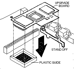
- Remove any installed Math-Co (and also any math-Co empty socket)
- Install plastic guide and plastic insert on planar.
- Insert any removed PLCC Math Copro into 486SLC3 Processor Upgrade board in U1.
- Install Upgrade board until pins are fully-seated, and edge-snaps click into place.
|
Features and Performance Enhancements
- The processor operates at three times the speed of the base system planar.
It supports 20 and 25MHz speeds, with the achieved processor speeds are 60MHz
and 75MHz respectively.
- The CPU includes an internal memory cache controller and 16KB memory cache.
- The combination of triple clock speed, integrated cache and optimized
instructions provides sizable performance improvements.
- You can address up to 16MB of memory with this.
|