|
Source: PC Mag May 26, 1992
Author: Douglas Boling
In the previous issue we reviewed the basic concepts of serial
communications. This time, we'll discuss their specific implementations in
today's PCs.
To provide for the full needs of a serial port, including the associated
control lines for RS-232 communication, requires the services of a chip called
a Universal Asynchronous Receiver/Transmitter (UART). The processor controls
the UART by writing to its registers. The National Semiconductor INS-8250 UART
was used in the original PC, and its register set has become the de facto
standard for all serial ports on PC compatibles.
The starting address for the UART I/O ports will vary with the COM port
being used. The original PC and PC-XT specified two serial ports, the first
starting at I/O address 3F8h and the second port at I/O address 2F8h. The IBM
PS/2 Hardware Technical Reference specifies eight possible serial ports with
corresponding register locations. The PC BIOS keeps a list of the base
addresses for the first four serial ports in the BIOS data area, starting at
address 40:0h.
Sending data out through the serial port is a simple matter of writing the
data bytes to the UART's Transmit Data register. Data the UART receives is made
available to the processor in the Receive Data register. The CPU can poll the
UART to determine when to read or write data to it, or, for maximum efficiency,
the UART can be programmed to interrupt the CPU when data needs to be written
or read.
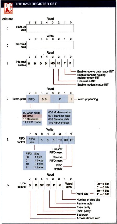
Figure 1: There have been three major
revisions of this register set. Dark blue indicates the changes that resulted
from the first upgrade, the 16450 and 8250A chips. Light blue shows the
revisions that accompanied the 16550. Pink shows the changes introduced with
the IBM Type 3 serial port. Addresses 0 and 1 are also used for the Baud
Divisor Latch Register.
The register set for the 8250 family of UARTs is shown in Figure 1. There
have been three major revisions of this register set, all backward-compatible
with earlier versions. The different shadings in the figure indicate which
registers are included in each version. The figure also shows the functions of
the individual bits in each of the registers, as well as their offset from the
base address of the UART.
The Transmit Data and Receive Data registers are the first members in the
8250 set. If the processor writes a value to the Transmit Data register, the
8250 will immediately copy the data into an internal register and shift it out
the transmit line of the serial port. The Receive Data register returns the
last data to be received on the Receive Data line of the serial port. Note that
if the Receive Data register is not read before the next byte has been
received, the byte currently in the Receive Data register will be lost. The
8250 detects this condition and sets the overrun bit in the Line Status
register.
The 8250 can be programmed to interrupt the processor when data needs to be
read from the Receive Data register or written to the Transmit Data register.
The Interrupt Enable register determines the conditions under which the UART
will interrupt the processor. Specifically, the chip can be programmed to
interrupt when it needs data, when the modem-status lines change, or when an
error condition is detected. The modem-status interrupts occur whenever the
Data Set Ready (DSR), Clear to Send (CTS), Data Carrier Detect (DCD), or Ring
Indicator (RI) line has changed.
The error conditions detected are framing errors, parity errors, overrun
errors, and break detection. When the processor reads the Interrupt
Identification register, the reason for an interrupt can be determined. The
primary control register for the 8250 is the Line Control register. The bits in
the Line Control register control, among other things, the size of the data
word, the number of stop bits, and the parity configuration. The data word size
can be configured from five to eight bits, and one or two stop bits can be
selected. Odd, even, or stick parity can also be set.
Bit 7 of the Line Control register controls access to the Baud Rate Divisor
registers. When this bit is 1, the I/O address that normally accesses the
Transmit Data and Receive Data registers and the Interrupt Enable register
accesses the Baud Rate Divisor register instead.
The Baud Rate Divisor register is a 16-bit counter that determines the speed
at which the 8250 transmits and receives data. To set the baud rate on a PC,
the 8250 is driven by a 1.8432-MHz clock. With each clock cycle the Divisor
register is decremented by one count. When the Divisor register reaches 0, the
counter is reset and one bit of data is transmitted to or received from the
UART.
Different baud rates can be set by placing different values in the Divisor
register. A value of 96 (60h) in the register causes the 8250 to operate at
example. Putting a value of 1,200 baud, for 12 in the Divisor register will
result in a baud rate of 9,600. While the original PC only supported baud rates
up to 9,600, the baud rate can be set to a maximum of 115,200 by using a
divisor of 1. Note that the baud rate and bps rate are the same in a purely
digital circuit such as that of the UART.
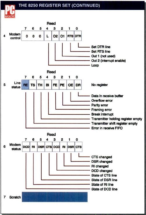
Figure 1: There have been three major
revisions of this register set. Dark blue indicates the changes that resulted
from the first upgrade, the 16450 and 8250A chips. Light blue shows the
revisions that accompanied the 16550. Pink shows the changes introduced with
the IBM Type 3 serial port. Addresses 0 and 1 are also used for the Baud
Divisor Latch Register.
The Modem Control register allows the processor to set the RS-232 control
lines that link the computer and modem. Bits 1 and 0 control the state of the
modem's Request to Send (RTS) and Data Terminal Ready (DTR) lines. Bit 4 of
this register loops the output of the transmitter back into the receiver,
allowing the CPU to test most of the UART circuitry. Two general-purpose lines,
Out 1 and Out 2, are provided. Out 1 is not used for PC serial ports, but Out 2
provides an additional control over the serial interrupt. The Out 2 bit must be
set if the UART is to interrupt the processor, regardless of the state of the
Interrupt Control register.
The Line Status register lets the processor read the state of the UART. When
in a polling mode, the processor reads this register to determine when to read
or write a byte of data from or to the UART. Any error conditions in the UART
are also indicated in the Line Status register. The Modem Status register can
be read to determine the state of the DCD, RI, DSR, or CTS line. The register
also contains bits that are set when the state of any of those lines changes.
This allows the processor to determine whether any of the lines has changed
state since the last time the register was read.
UART UPGRADES
The first upgrade on the 8250 was the 16450 UART, used in the PC AT. The
16450 provides a faster interface between the UART and the processor, but its
only functional difference from the 8250 was the addition of a scratch register
where the processor could store a byte of data. The PC Convertible, IBM's first
laptop computer, used an 8250A, which is functionally identical to the
16450.
With the release of the PS/2 models in 1987 came the 16550 UART. Here the
story gets a little muddy. The original PS/2 Models 50, 60, and 80 used an
early version of the 16550 with a bug that disabled its main feature: a set of
FIFO (first in, first out) queues that would have dramatically improved serial
performance. The 16550 was replaced by the 16550A in the PS/2 Model 70. This
fixed the bug in the FIFO section of the chip: improved versions of the Models
60 and 80 also use the 16550A. But the only way to determine if the 16550s in
the PS/2 can use the FIFO queues is to test the serial chip. To confuse matters
further, while improved versions of the PS/2 Model 50 incorporate the 16550A,
IBM does not support using the FIFO queues on the Model 50!
The FIFO queues of the 16550A represent a significant development for serial
communications. Faster serial-port and modem speeds mean that the CPU must
spend more and more of its attention servicing the UART. For example, while the
processor must read the UART every 6 milliseconds for a serial port at 1,200
baud, it must read the UART every 83 microseconds at 9,600 baud. This increased
load is compounded by multitasking operating systems such as Enhanced-mode
Windows and OS/2. In a multitasking operating system, the computer may be too
busy to service the serial port.
This is where the FIFO queues come in. The queues consist of small buffers
that hold up to 16 bytes of data. After filling the transmit FIFO queue with 16
bytes of data, the processor will not bother with the serial port again until
all 16 bytes have been transmitted. The receive FIFO queue works the same way.
When the 16550A UART needs service, the processor can read the last 16 bytes of
data received. By using the FIFO queues, a 16550A UART running at 9,600 baud
needs only the same service time as a 16450 UART running at 600 baud.
One additional register and several control bits have been added to the
Interrupt Enable and Interrupt ID registers in the 16550A. The additional
register is the write-only FIFO Control register. This register enables the
transmit and receive FIFO queues, clears the queue contents, and sets the
interrupt trigger level of the queues.
The 16550A can be set to interrupt the processor when the receive FIFO queue
holds 1, 4, 8, or 16 bytes of data. Although the processor is interrupted when
the appropriate level is reached, the UART continues to store its data in the
FIFO queue. This allows the operating system enough time to complete its
current task before having to service the UART.
The Interrupt ID register in the 16550A UART has been expanded to encompass
interrupts from the FIFO queues. Bits 6 and 7 indicate whether the UART is in
FIFO mode. Bit 3 indicates that the interrupt was caused by a character
time-out condition in the receive FIFO queue. This interrupt allows the
processor to read the last few words in a serial transmission when there are
not enough data words received to trigger a FIFO full interrupt.
Using the FIFO queues in a serial communications program is really quite
simple. Once initialized in FIFO mode, the UART will wait until the FIFO queue
is full before interrupting the processor for service. The interrupt routine
repeatedly reads the Receive register until the queue is empty. On the transmit
side, a communications program writes enough words to the UART to fill the
transmit FIFO queue. The UART will then not need data to transmit until the
transmit FIFO queue has been exhausted.
To determine whether the UART in a computer contains usable FIFO queues, a
program only needs to set some bits in the UART register and check the
response. The assembly language routine, SERTYPE, in Figure 2 determines if the
FIFO queues are available.
SERTYPE Routine
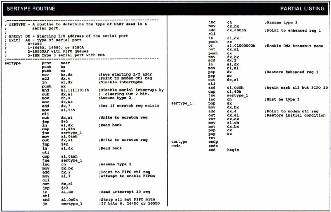
The routine in Figure 2 first sets bit 0 of the FIFO Control register and
then reads the Interrupt Identification register. If bits 6 and 7 are both 0,
the UART is a 16550 and the FIFO queues should not be used. If the bits are
both 1, the UART is a 16550A and the queues can be used.
If the 16550A is detected, the PC identification bytes are checked to see if
the computer is a PS/2 Model 50. If it is a Model 50, the routine indicates
that the FIFO queues are not found, since this PC does not support FIFO mode.
The routine then goes on to check for the presence of an enhanced DMA serial
port. The new DMA serial port is the latest and most exciting development in PC
serial ports.
DMA SERIAL PORTS
The improvements provided by FIFO queues can be significantly augmented by
adding DMA support to the serial port. DMA support does more that just dump
serial data into a buffer; it can scan the incoming data for special
characters, and it can even provide its own flow control. On the IBM side, the
new PS/2 Models 90, 95, and 57 incorporate the enhanced DMA serial ports, and
other manufacturers either have done so or will.
The enhanced serial port also breaks one of the historic PC barriers by
allowing the use of a faster baud clock. By setting a bit in one of the
enhanced registers, the standard 1.8432-MHz clock can be switched to 11.0592
MHz. This raises the theoretical serial rate to 691,200 bits per second. As
with earlier serial ports, the IBM models do not support the highest possible
speed, but they set their limit at 345,600 bps, which is still very fast.
One of the difficulties of providing DMA support for a serial port is the
need to scan for control characters among the received data. Normally, this
process uses the CPU to compare a received data byte with a set of known
control characters. With the DMA feature active, however, the processor may not
read the received data until the DMA buffer is filled.
To avoid any wait for processor service, the enhanced serial port has
compare registers that can be used to check for up to three special control
characters. When such a character is found, the UART can be programmed to start
or stop transmitting automatically, to delete the character, to interrupt the
processor, or any combination of these events.
The new DMA serial port (a Type 3 serial port, in IBM lingo) is backward
compatible with the earlier 8250 family of UARTs. While all previous registers
are present, an entirely new set of registers has been added to control the
enhanced features. The new registers are accessed by adding 8000h to the base
address of the start of the conventional UART register set. For example, if a
serial port normally starts at I/O address 3F8h, the enhanced register set will
start at 83F8h. Figure 3 shows the new registers used by the Type 3 serial
port. Their description will serve as something of a programmers'
reference.
IBM Type 3 Expanded Register Set
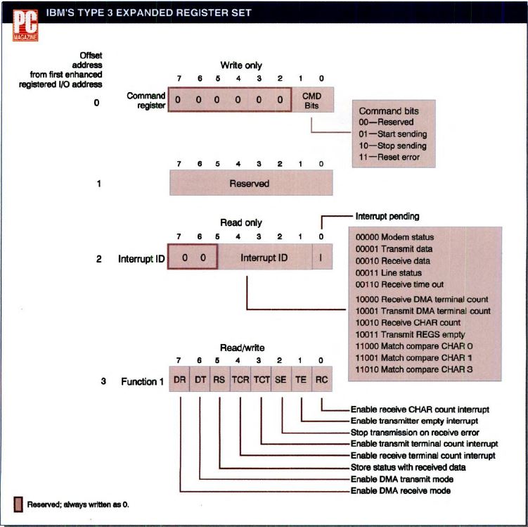
Figure 3: The DMA serial port, or Type
3, is backward-compatible with the earlier 8250 family of UARTs. This
illustration shows the new registers used to control the enhanced features,
such as flow control and a faster baud clock.
The first of the enhanced registers, the Command register, controls the
transmission of data in DMA mode. Data sending can be stopped and restarted,
and any error conditions can be reset using bits 1 and 0 of the register. All
of the other bits in this register are reserved.
The Interrupt ID register identifies all interrupts that can occur in both
conventional and enhanced modes. In enhanced DMA mode, new sources of
interrupts include Terminal counts on the transmit or receive DMA controllers
or a compare register match on the received data.
Enhanced Function Register 1 controls the enabling of the DMA modes of the
UART. This register also enables interrupts for the serial port, including DMA
terminal count notification. Bit 5 of this register forces the UART to store a
byte of status information with every byte of received data. By enabling this
mode, you can half the number of data bytes that can be kept in the FIFO and
DMA buffers, but it allows the processor to check the status of each data byte
when it reads the DMA buffer.
IBM Type 3 Expanded Register Set (continued)
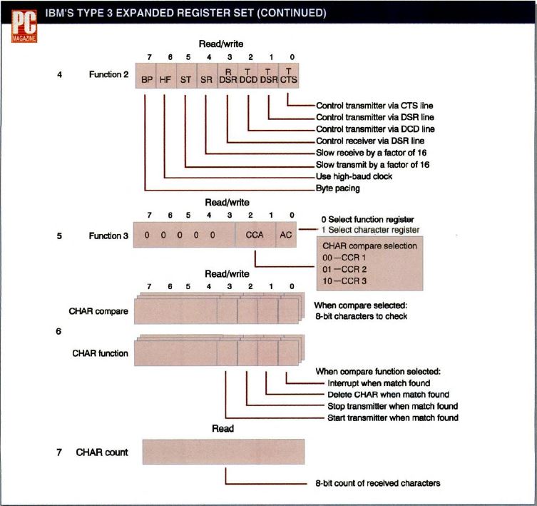
Enhanced Function Register 2 controls the baud clock and enables hardware
flow control. Bit 7 paces the transmit rate, using the Receive Count register.
Bits 5 and 4 cut the transmit and receive rate of the UART by a factor of 16,
slowing the UART so that slower processors can keep up with the serial port.
Bit 6 of this register determines whether the 1.8432- or 11.0592-MHz baud clock
is used. Finally, the lower four bits of this register determine the hardware
flow control of the serial port. When these bits are set, the UART will stop
and start transmitting and receiving in accordance with the DSR, DCD, and CTS
status lines.
Enhanced Function Register 3 controls access to the character compare
registers. Bits 2 and 1 select which of the character compare registers is
accessed. Bit 0 selects the character compare register or its accompanying
character function register. The character compare register is the actual 8-bit
byte to check. The character compare function register selects which event
should occur when a matching character is found.
After setting the Enhanced Function Register 3 to access the proper
character compare register, that register can be read and written at that
character compare register address. If a character compare function register is
selected, only bits 3-0 are used. More than one event can be programmed for
each character match by enabling multiple events in a Character Compare
Function register.
The final register in the enhanced register set is the Receive Character
Count register. This register has two functions. The first is to keep a tally
of the bytes received by the UART. The other is to act as a pacing register for
transmitting data. When in the pacing mode, the UART slows transmission of data
by dividing the baud clock by 256 times the value in this register.
The FIFO queues and DMA interface that enhance the performance of serial
communications have their counterparts in the world of parallel ports, which
will be the subject of a future Lab Notes.
Douglas Boling is a contributing editor to PC Magazine.
Putting Serial-Port
Technology in Perspective, Part 1
|