|
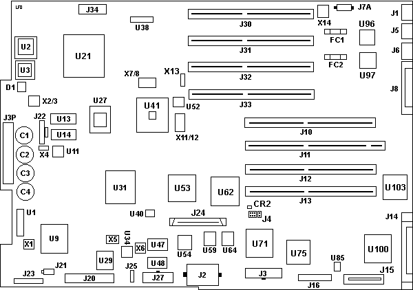
7012-397 Planar
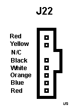
J22 Keylock Pinout
7012-397 Planar

C1-4 12,000 µF, 6.3 V, 105 °C
CR2 SCSI LED
D1 Motorola R7 20 B2515L
FC1,2 5MP 800 mA 250 V
J1 Keyboard port
J2 I/O Power connector
J3,27 Power connector
J3P Unused power connector, 24-pin
J4 ?
J5 Mouse port
J6 Tablet port
J7A Rear Fan
J8 Parallel port
J10,12,13 32-bit MCA slot
J11 32-bit MCA slot w/ AVE
J14 External SCSI-2 mini-C68
J15 Ethernet PHY slot
J16 Serial port header
J20 Floppy connector
J21 Battery, Panasonic 3 V BR-E5 Lithium
J22 Key Mode Switch / Reset Button
J23 LED display
J24 Internal SCSI "P" connector
J25 Power Control
J30-33 Memory Card Slots H, D, B, F
J34 Unused 16-pin header
U1 07L7258-SER Network address
U2 93H7791
U3 07L7256 CPUID=94
U9 65G7530
U11 NS DP8570AV Timer Control Periph.
|
U13,14 Hitachi HM514280AJ7
U21 88H2265 Power2 Super Chip
U27 50G6947
U29 NS DP8473AV Floppy controller
U31 Toshiba 81F8125 TC140G44AF
U34 73H2565 Turbo
U38 51G9835
U40 PTC resistor, internal SCSI bus
U41 26H6184
U47,48 Hitachi HM628128BLFP-7
U52 Motorola MC12429
U53,100 82G2645 SE SCSI ctrl. "Cutlass"
U54 AMD AM186 EM-40VC (SCSI)
U59 88G1094 SCSI BIOS Even ???
U62 61G2323 MCA Bus iface "Malibu" (SCSI)
U64 88G1095 SCSI BIOS odd ???
U71 81F8150
U75 intel KU82596DX25 LAN co-pro
U85 PTC resistor, external SCSI bus
U96 N82C55A2
U97 80C51BH
U103 NS PC16553DV
X1 24.0000 MHz osc
X2/3 16.000 MHz osc
X4 32.768 kHz
X5 40.0000 MHz osc
X6 14.3181 MHz osc
X7/8 3.906250 MHz osc
X11/12 40.1500 MHz osc
X13 16.000 MHz osc
X14 9.21600 MHz osc
|
J22 Keylock Pinout

|
The red wire only connects the end pins.
Reset switch leads Yellow and Black. (C&K 8168)
Keylock switch leads Orange, White, Blue. (C&K N Series)
Maint: Orange - White
Secure: Blue - White
Normal: All open
|
Remove Card Guide Frame
There's a hard and an easy way. To save time, the easy way is to remove both
fans by unscrewing the four gold colored screws on the top of the card guide
and sliding the fans (still in their metal mounts) up and out of the card
guide.
Now all three mounting screws are visible AND accessible. Remove all three
screws and lift the card guide out.
Install Card Guide Frame
One way is to just start the three gold mounting screws into the case. Place
the frame just to the rear of the screws and slide it forward until the frame
is seated against all three screw. Now tighten them down. Reinstall the
fans.
Remove and Install P2SC Heatsink
The best way to do this is with the planar out of the case, otherwise the
front outer nut is hard to start by hand. Note:
Align the heatsink fins so that they are parallel to the air flow. In other
words, so the air can blow in between the fins.
Remove Planar
Remove front card guide frame. Unplug rear fan, remove memory card rear
guide, pull fan off rubber mounts. Unplug all planar power and signal
connectors. Remove the parallel port and external SCSI port posts. Remove all
planar mounting screws.
Pull planar towards front of case until the ports clear their case cutouts
at the rear. Pivot rear of board up and forward until you can remove it.
Memory
The S.6 memory card illustration is
HERE.
The memory modules for Model 397 must be installed either in pairs (2 cards)
or quads (4 cards). Each card in a pair or quad must be of equal capacity. If
only a pair of memory modules is installed, use slots D and H. If a quad is
installed, use slots B and F, in addition to slots D and H.
|