|
rf90952a.exe Reference Disk Type 2 Processor Complex v1.21 (zipped image)
rd9095a.exe Diagnostic Disk Type 1 - 4 Processor Complex v2.33 (zipped image)
192-100 IBM PS/2 486-25/50 Microprocessor Upgrade (CPU only!)
192-099 IBM PS/2 486DX2-50 Processor Upgrade
486 Interposers and Upgrades
Specifications
Memory
Features
Complex Origins
"H" and "L" Complex Identification
"H" / Upgrade 486SX 25 MHz
"L" / Upgrade 486DX2 50 MHz
Rear of "H" / "L"
J1 Jumper
U6 Variants and Kingston Turbochip
Running DX4-100 on L (Requires U23)
3172-002 "H" complex 93F1666
Overclock attempt
ODP vs. ODPR
ODP in Original Socket
In Defense of the L
System Firmware
ROM Images
Support for >1 GB Disks as IML Drive
Known Problems
171 POST Errors
Diskette Data Loss
16-bit Busmasters
Japanese 486SX 25 MHz / 486DX2 50 MHz Complex
Japanese DX2-66 Upgrade Type A Complex (unique!)
Japanese DX2-66 Upgrade Type B Complex
Specifications
Memory
RAM
- Min/Max on system board: 8 / 64 MB, 16 MB addressable by DMA
- PS/2 70 ns parity 72-pin SIMMs, 85 ns SIMMs not supported
ROM
Cache
- L1: 8 KB (486 SX, DX2)
- L2: none (no socket for cache)
Features
- No Level 2 cache socket on complex.
- H models socketed for a 487 copro or a 486DX2 50 MHz upgrade chip.
- High speed 25 MHz DMA - now synchronous with 486; 24-bit DMA. *
- Faster bus arbitration (than Base 1) for better busmaster performance.
- Memory controller supports both interleaved (higher performance
pairs of SIMMs) and non-interleaved memory (allows single SIMMs).
- 20 MB per second data transfer support (for MCA bus).
* - The same DMA controller chip is used in other systems that support
32-bit DMA (namely the Type 3 complex,
85 X planar,
85 K/N planar, and other. So is this a case
of a 32-bit part being limited to 24-bit by the board and/or firmware
implementation?
Complex Origins
The Type 2 complex was most likely designed by IBM Japan. This is supported
by the following facts:
- The core logic consists of Japanese gate arrays (QFP package)
- The PCB itself looks very similar to the other boards that were designed by
IBM Japan. Namely - solder trap pads for wave soldering (on the backside),
silkscreen in the more descriptive "position/type" format, etc.
- The firmware has support for the
PS/55 Model 5560 planar
(Planar ID F9FE).
"H" and "L" Complex Identification
Both H and L have no L2 cache socket or solder pads for one.
H models (92F0079) came with a 486SX-25 in U8 and have a second socket (U9)
for a 487 copro or a 486DX2-50 ODP upgrade chip. They will accept a Turbochip
if the DMA controller is the good one.
L models (92F0161) came with a 486DX2-50 in U8 and have only solder pads at
the U9 location. They will take a ODPR or (with the good DMA controller) a
Turbochip.
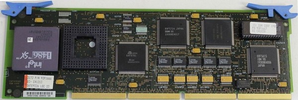
"H" / Upgrade 486SX 25 MHz 92F0079, FCC ID ANOIBM486SXB25
![[P]](/other/img/photo.gif "Front") |
|

U5 (GA-J) 89F5724 Memory Controller
U6 (GA-M) 92F1428 DMA Controller
U7 07G0463 BIOS ROM Am27C010-155DC
U8 169-pin LIF CPU socket (486SX-25)
|
U9 487 socket
U10 (GA-T) 64F8781 Memory Data Buffer
U16 (GA-R) 89F5415 MCA Buffer/Controller?
Y1 50.0000 MHz osc (half can or SMD)
|
Note: There are two slightly different versions of
the PCB. The most noticeable difference on the front side is the unpopulated
position U38 - the older revision has pads for a square PLCC-20/28 package
while the newer one has two rows of pads for a SOIC-16/20 package.
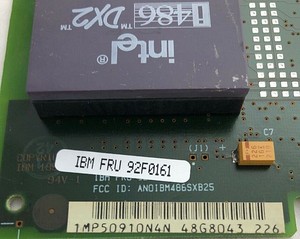
"L" / Upgrade 486DX2 50 MHz 92F0161, FCC ID ANOIBM486SXB25

U5 (GA-J) 89F5724 Memory Controller
U6 (GA-M) DMA Controller
U7 BIOS ROM Am27C010-155DC
U8 169-pin LIF CPU socket (486DX2-50)
|
U9 Solder pads for 487 socket
U10 (GA-T) 64F8781 Memory Data Buffer
U16 (GA-R) 89F5415 MCA Buffer/Controller?
Y1 50.0000 MHz osc (half can or SMD)
|
Rear of "H" / "L"
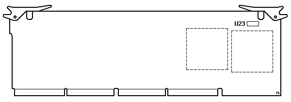
U23 74F08 (SOIC-14) or pads for SOIC-20
(see note below and also info about running DX4).
Note: There are two slightly different versions of
the PCB. On the back side there is one significant change - on the older
version position U23 is unpopulated (SOIC-20) on the newer one there's 74F08
(SOIC-14) in the same place.
J1 Jumper
Right below the CPU socket there are pads for a 2-pin jumper marked as
"(J1)". What is it for?
U6 Variants and Kingston Turbochip
Some Type 2 (92F0079) suffer from an "incompetent DMA-chip",
which is P/N 92F1428 at position U6 on the card. Working Type 2s 92F0079 have
a DMA-chip P/N 10G7808 at U6. If U6 is 10G7808 Kingston Turbochip should work
fine. The earlier Type 2 use the 92F1428 - which ends the experiment in
odd results (permanent I9990044, 605, 165 errors, and inability to read
from FDD). Known U6 variants:
- P/N 92F1428 (Bad)
- P/N 10G7808 (Good)
- P/N 10G4714 (Possibly Good)
Running DX4-100 on L (Requires U23)
Jay Bodkin said (edited):
I got a bizarre thing happening on my 8595 Type 2. I upgraded the
CPU from an Intel 486 DX2-50 to 486 DX4 -100. (I got the U6 P/N 10G4714). The
machine boots with the reference disk and it detects that the processor complex
has changed. The front panel has the usual code to go with that. Then it asks
to perform automatic configuration, to which I replied y. Next, it complains
that there are still unresolved configuration errors, and wants a reboot. After
another reboot the front panel displaying 9600-8N1 and refuses to boot
further.
Peter Wendt replies:
OK, so at least you're not in danger toasting the CPU. (Tastes
pretty bad anyway - toasted or raw) FWIW: I ran the Kingston Turbochip-133 at
100MHz on various 25MHz Type 2 platforms, but all of them had the "competent"
DMA chip 10G7808 at U6/GA-M *and* had the latest platform BIOS 41G9361.
All "L" complexes have U23.
Complex PCB is 06G6870, BIOS 07G0463, DMA 10G7808, sticker 48G8043
Complex PCB is 06G6870, BIOS 41G9361, DMA 10G4714, sticker 06G7009
"H" complexes with 48G8042 on sticker below CPU have U23
Complex PCB is 06G6870, BIOS 07G0463, DMA 10G7808
"H" complexes with 07G3152 on sticker below CPU do NOT have U23
Complex PCB is 06G4561, BIOS 07G0463, DMA 92F1428
The presence of a 74F08 chip at position U23 (on the
solder side of the board) seems also be a critical point: if it is there the
board is made in 1992, earlier 1991-manufactured board lack this chip - and
failed to work with anything faster than a DX2-25/50 (Or a DX2-33/66, which
will run as a 25/50 there only anyway). DX4s or Evergreen, Kingston and such
like based on a quad-clocked AMD 5x86 failed with no exception on the earlier
ones.
There should be a silk-screened "Date of MFG" number somewhere on the
platform, like e.g. 2092A0700 - which means 20th week 1992 (first 4 digits). If
yours is a 1991 platform or early 1992 without the U23 chip - forget about it.
On these boards I had a failure-rate of 100% (about 20 out of 20...).
> Interestingly, putting back the 486 DX-2 50 doesn't work now either. It
still gets stuck on the 96-8N1, even after removing the battery for a couple of
minutes!
IBM wrote in the HMM "Remove the battery, then wait 5 minutes..." (HMM,
September 1993, P/N 71G9316, page 300, "96 8N1 Error Message") but empirical
research showed that this doesn't work fairly often.
Shortening the battery connectors (with the battery removed of course) *and*
toggling the startup password jumper seems to be the only fast cure. There
seems to be a board logic, that ANDs the two conditions after a power-on and
deletes the entire setup from the CMOS.
At least during the "hot phase" when the Mod. 90s and 95s can be found in
larger amounts at the customers this procedure was the only one that worked in
a sufficiently fast way. And I had quite a lot 95s under service... ;-) (Some
are mine now)
3172-002 93F1666
The 3172-002 uses a 95 single serial planar and an "H" complex with a 3172
flavor complex BIOS (93F1667). This particular 3172-002 complex is the later
version with a 10G7808 DMA controller and U23 on the back. They will happily
accept the 41G9361
BIOS.
Overclock attempt
Swapping a 66.667 MHz osc in for the 50 MHz one will result in a 00010200
code in the upper left hand of the screen and a system hang. The Y1 Oscillator
drives both the data bus and the DMA controller. 0001 02XX ROM checksum or
timer error.
ODP vs. ODPR
The 169-pin is the ODP-version - substitutes a 487SX with the 486SX still in
place. Important on boards with soldered CPU or a second socket.
The 168
pin is the ODPR-version, where the -R- stands for "Replace"... it replaces the
486SX / 486DX respectively and does not need the "SX-disable" pin
therefore.
ODP in Original Socket
Dr. Jim, can the 169th pin be bent/removed and the CPU used?
Yep. The socket I just put into my P75 has an empty hole to allow that extra
pin to pass. I've drilled similar holes in older 486 sockets myself. Carefully.
BTW, I've been informed that it is NOT the SX disable pin, just a key pin. The
SX disable is elsewhere.
Jose Duran:
You are right, this pin is only a key pin without any signal. The
SX disable pin is B14 (as far as I remember). I have installed an AMD DX5 on an
upgrade socket with a voltage adapter. Since my CPU didn't have any SX disable
signal on it. I had to solder a wire from pin B14 to ground, thus putting the
SX into tristate. It works perfectly.
In Defense of the L
Actually Tony Ingenoso said:
Austin DID do some LAN server performance modeling along these
lines and determined that there WAS a gain to be had from a dual 386 machine as
a 386 file server could become CPU bound. Once a 486DX-33 was fitted, even the
heaviest traffic hitting the server wasn't enough to saturate the DX33 in a
pure file server role.
My own casual observations of the lowly (and IMO brilliant) DX2-50 T2
complex validated Austin's results. With all NT4 Server's performance
monitoring turned on I was never unable to saturate the stock CPU on a 9595-0LF
in a pure file server role. It might run up to 80%, maybe even peak to 90%, but
it never became saturated at 100%. This was with several other PC hammering it
over a 16mb T/R LAN. Operating within its design purpose, doing what it was
sold to do -- a stock T2 was is a word "sufficient" to the task in all
respects, and remains so even today when run in a pure file server role.
The problem is that TODAY, we are asking these machines to take on more than
they were intended to do initially. Modern "desktop" usage has a dramatically
different use profile than pure file servers have, and it shows. GUI's are a
big drag on performance, and the 95's placement of the video on the bus hurts
quite a bit as well.
System Firmware (POST & BIOS)
Simplified firmware stored in EPROM. IML image required for the system to operate.
ROM Images
All ROMs are 27C010 or compatible (position U7).
07G0463 08 Aug 1991, rev. 0, Type 2 (early "H"), seen mostly with 92F1428 DMA Ctrl.
41G9361 03 Mar 1992, rev. 3, Type 2 ("H" or "L"), stock on Hs with 10G7808 DMA Ctrl.
Support for >1 GB Disks as IML Drive
Type 2 complexes require the combination of
BIOS 41G9361 and SCSI
BIOS 92F2244/45 in order to handle IML drives >1GB (new limit is 3.94GB).
The upgrade BIOS incorporates the "Enhanced IML" which supports IML from a
drive >1GB and "Search IML" which allows IML from a drive other than ID6.
The SCSI BIOS 44/45 pair supports drives well over 8GB. (Ed. You OS may have
other ideas...)
The old' complex ROMs' IML support somehow does not make (proper) use of
"Enhanced IML", possibly due to bad bit-shifting and/or masking when
translating the cylinder/head/sector information to and from the SCSI "logical
block/sector" value.
More information HERE.
Known Problems
171 POST Errors
Symptom: A 00017100 (171) error occurs on POST (Power-On System
Test). This problem may occur on 8595/9595 models xLx or xHx systems during the
installation of a LANStreamer MC32, MC16 or EtherStreamer MC32 in slot 8.
Fix: Do not install any of the above referenced adapters in slot 8.
Relocate the adapter to one of the other Micro Channel slots. No further
engineering action is planned.
Diskette Data Loss (ECA100)
This problem may allow bad data to be read from or written to a device
WITHOUT any error indications or other evidence of system failure. This affects
any device attached to the floppy controller that is "seen" as a floppy drive,
such as some tape backup devices.
Affected Systems: All systems using the 486SX/25 MHz complex FRU
P/N 92F0079.
Notes: The following are no longer supported:
5.25" Diskette Adapter/A (6451007), 4869-001 360 KB and 4869-002 1.2 MB
External Floppy. These adapters use a separate device driver (not BIOS), and
DMA verify. Updating the system partition will NOT cure the problem.
16-bit Busmasters
When installed with the 486SX/25 Processor Upgrade Option, 16-bit bus
masters (for example, PS/2 Micro Channel SCSI Adapter (#1005, 6451109)) that
support 32-bits of addressing will cause system malfunction and/or potential
loss of data when the user installs greater than 16 MB of system memory.
| 
