|
rf90951a.exe Reference Disk Type 1 Processor Complex v1.31 (zipped image)
rd9095a.exe Diagnostic Disk Type 1 - 4 Processor Complex v2.33 (zipped image)
SCSIFIX.ZIP Finally! A utility to
alter the number of sectors for a SCSI drive and convert them to a 3.94 GB
drive! Bob Eager, you have answered a prayer!
Upgrading the Type 1 Complex
Specifications
"G" 486SX 20 MHz
J2 Functionality
"J" 486DX 25 MHz
"K" 486DX 33 MHz
What is the Square Of Death?
Square of Death Limits
ECA #0530 90-0K9/95-0KD with Complex P/N 84F9356
Upgrade 486DX2 66 MHz
Upgrade 486DX 50 MHz
Info on Weitek 4167
256 KB Cache Memory Option Kit
256K 17 ns Cache Daughtercard
256K 15 ns Cache Daughtercard
L2 Cache Performance
ODP vs. ODPR
System Firmware
ROM Images
Support for >1 GB Disks as IML Drive
Enhanced BIOS Effects
Upgrade EPROM Additional Capabilities
Complex EPROM Speeds
Am27C010 versus Am28F010
Type 1 Complex Upgrade to "8590/95 Dual Booting Capability EPROM"
Data Buffers
CR1 Diagnostic LED
Japanese 486DX 25 MHz Complex
Japanese 486DX 33 MHz Complex
Specifications
Memory
RAM
- Min/Max on system board: 8 / 64 MB
- PS/2 parity FPM 72-pin SIMMs, interleaved (install SIMMs in pairs)
- 80 and 85 ns memory SIMMs are supported, 70 ns for optimum memory performance.
ROM
Cache
- L1: 8 KB
- L2: optional 256 KB write-through (except SX-20 "G",
standard with Upg. DX-50)
- Both caches are arranged in lines of 16 bytes:
- 512 lines for the internal cache
- 16384 lines for the optional cache
Features
- Socket for 17 ns 256 KB write-through L2 cache on J, K, and Upgrade DX2-66
- Socket for 15 ns 256 KB write-through L2 cache on Upgrade 486DX-50
- No Weitek 4167 coprocessor socket on later J, K, and Upgrade complexes
- 24-bit DMA; 10-12 MHz *
- Dual path memory design (Dual Bus Interleave).
- 20 MB per second data transfer support (for MCA bus)
* DMA controller originally limited to 16 MB. Fixed by the last BIOS update
(unknown how).
Ed. Where is the Micro Channel controller on the
Type 1? Implemented using PALs and 74xx TTL chips?
"G" 486SX 20 MHz
FRU P/N 92F0049 (486SX) or 92F0065 (487SX), P/N 92F1413, FCC ID ANOIBM486A20
![[P]](/other/img/photo.gif "Front")
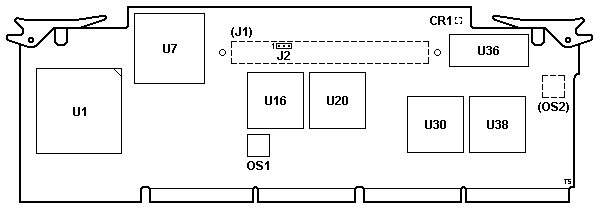
CR1 Solder pads for LED
J1 Pads for L2 cache connector
J2 486SX/487SX jumper
OS1 20.0000 MHz osc
OS2 Pads for osc
U1 169-pin LIF CPU socket (486/487SX-20)
|
U7 57F2194 Memory Controller
U16,20 78F1659 Data Buffer (RAM)
U30 78F1659 Data Buffer (MCA)
U36 Am27C010 BIOS ROM
U38 63F7520 DMA Controller
|
J2 must be set to 1-2 if a 487SX
processor is installed in position U1. If there isn't a 487SX in U1, the jumper
must be on 2-3.
Note: When installing a CPU, align beveled corner
with the beveled outline on the board.
Note: The "G" is the only Type 1 complex to lack a
160-pin L2 Cache option connector.
J2 Functionality (MAJ Tom's SWAG)
The jumper most likely just signals the glue logic (PAL/74xx) to swap the
two (?) signals that are assigned differently on the 487SX SKU (pinout
comparison HERE).
Intel reassigned the pins (and added a mechanical key) to prevent people from
using the 487SX "FPU" as a standalone processor instead of the more expensive
486DX SKU. Intel's design had two sockets and the original 486SX would stay in
its place when the 487SX chip was installed in the upgrade socket. But IBM
probably didn't like this approach because it required extra board space,
higher current draw, and more heat. Instead they added a jumper to switch
between the two pinouts, as did many clone boards. But unlike the clone boards,
IBM's G complex was probably ok in Intel's eyes because the customer had to pay
for both chips - the 486SX SKU when they originally bought the complex/machine
and the second (cheaper than DX) 487SX SKU when ordering the upgrade. IBM never
offered complex boards without the CPU installed, AFAIK. At least not to the
end customer. The pesky clone board makers, on the other hand...
The Japanese Type 2 complex uses higher integration
and drops some features. This means more space on the board and also a lower
current draw and TDP, making the two-socket approach much more viable.
"J" 486DX 25 MHz
FRU P/N 64F0201, P/N 84F8036 (old) or 84F9432 (old), FCC ID ANOIBM486A25
191-052 IBM PS/2 486/25 AND 486/33 PROCESSOR UPGRADE OPTIONS

J1 The 160 position connector is AMP
650756-1, dtd 9145.
U8 The "J" complex has been seen in three guises:
- U8 present - 142-pin PGA socket for Weitek 4167; "SOD"
- U8 absent - socket solder pads only; "SOD"
- U8 absent - replaced by pads for PALs, delay lines, and a resistor network; "non-SOD"
"J" Variants
Looking into the functionality of a Weitek 4167 "Abacus" in the U8 position.
From this VERY limited sample, it seems you need 54F2958 Data Buffer
(old) in U16, 20, and 30 to support the Weitek 4167.
Special J (J with 4167 socket)
PCB 84F8036 026
Small sticker on Weitek socket "Kit 34"
Complex BIOS "IBM Confidential" U2IT16 84F9155 18 June 90
54F2958 Data Buffer (older?)
Not So Special J (4167 socket) Lorenzo Mollicone sent some pix,
84F8208 (handwritten on sticker)
BIOS 64F6032, 1990
54F2958 Data Buffer (older?)
Info on Weitek 4167
Weitek Abacus FPU by Axel Muhr
WeitekDisk.zip Test suite from Weitek (local link)
Applications that took advantage of the Weitek Abacus were
scarce. AutoShade, Autodesk Renderman, 3-D Studio were the
most prominent to use a Weitek coprocessor.
If you happen to own one, you might actually use or at
least test it... so here's the official test-suite from
Weitek. It contains these tools:
- DOS TSR to update the BIOS for Abacus support (if missing)
- Test tool - checks for Abacus presence using INT 11h BIOS calls.
- Diagnostic tool
- 2 demos: Side-by-side Mandelbrot benchmark and rendering Phong shaded beach ball
- Abacus macros for using it natively in your cool assembly code
copro16a.txt The best source of technical information
about the 4167 is the highly recommended copro16a.txt by Norbert Juffa in 1994.
4167 Floating-Point Coprocessor advanced data
"K" 486DX 33 MHz
FRU P/N 64F0198, P/N 92F2282 or 92F1197, FCC ID ANOIBM486A33
|
190-186 IBM PERSONAL SYSTEM/2 486/33 PROCESSOR UPGRADE OPTION
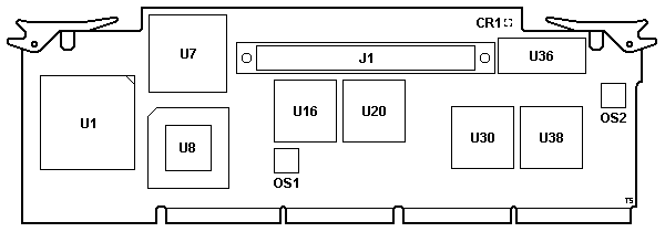
U8 The "K" complex has been seen in three guises:
- U8 present - 142-pin PGA socket for Weitek 4167; "SOD"
- U8 absent - socket solder pads only; "SOD"
- U8 absent - replaced by pads for PALs, delay lines, and a resistor network; "non-SOD"
"K" Variants
"Special K" (American breakfast cereal)
BIOS 84F9155 "IBM Confidential"
PCB is marked 64F5785 01 (right above U7)
54F2958 Data Buffer (older?)
Not So Special K
BIOS 84F9154 (unknown if 4167 flavored)
PCB is marked 64F5785 01
78F1659 Data Buffer
It appears they share the same PCB, one has "IBM
Confidential" / 54F2958, the other 84F9154 / 78F1659
(84F9154 likely a straight 486 BIOS)
Non-SOD Ks (Nothing where U8 was, just green resist)
FRU 64F0198
PCB is 92F1186 01
BIOS is 91F9812 (NOT Dual Booting Capability EPROM)
78F1659 Data Buffer
What is the SOD?
What exactly is this "Square Of Death" (SOD)?
David Beem responds:
The missing A1 & A2 pins make this a dead giveaway for the Weitek 4167 coprocessor. Steven Wachtel
reports "memory management" problems (ECA #0530) with the SOD complex, which
might make sense since the Weitek processors use high memory areas to transfer
op codes. So, can a socket go in place to see if a 4167 would be functional
there, or was it a dropped option? I suppose that with a couple SOD T1s (one of
each of the patches talked about in this thread) & a Weitek 4167 I am one
of those that could answer the question.
>Regarding the sensitivity of this complex, has anyone ever tried to swap
the BIOS with another Type 1 complex that is known to work with the faster
CPUs?
Despite the complexes being very similar & using the same reference
disk, fundamental changes for things like the Weitek coprocessor could really
mess things up. IBM would issue a whole complex if there were problems, not
just a BIOS change. Other than the T4 'N' I have seen no evidence of
other complex types checking things like CPUID.
SOD Limitations (from Tim Clarke)
The limitation of the 'poor DMA controller' for the Type 1 SOD board appears
to be that you can't run a Cyrix/IBM 5x86 at greater that 'x2 clocking' (i.e.
50 MHz in a Type 2, 66 MHz in a Type 1) or an AMD 586 at greater than 'x3
clocking' (i.e. 75 MHz in a Type 2, 100 MHz in a Type 1). Ed. You CAN run a 486DX4-100 ODPR on a SOD. It's only a
3x multiplier.
Not having a SOD Type 2 I can't test this, but I would expect the same
limits to apply. So, you should be able to run a DX2-50, DX2-ODPR (@ 50 MHz),
Cyrix/IBM 5x86 (@50 MHz) or AMD 586 (@ 75 MHz) in a SOD Type 2. The
'performance' of a Cyrix/IBM 5x86 @ 'x2 clocking' and the AMD 586 @ 'x3
clocking' are *roughly* equal, although I have a preference for the Cyrix/IBM
chip.
ECA #0530 90-0K9/95-0KD with Complex P/N 84F9356 (from Steven Wachtel)
These systems appear to have a memory management problem. In my environment
it was seen on a Model 90 with 16 MB of RAM. The system would hang during OS2
boot or during invocation of simple processes after a basic install (such as
the system editor). Symptoms at other OS2 sites would include excessive
"random" trap errors. Not using DOS on these systems, I would expect the
problem to surface as some indeterminate memory related failure in the E/XMS
region.
During initial setup of this machine, the problem appeared as an inability
to create a usable backup reference disk (if said disk was used there were
always errors). On restart after the failure the machine will request to exec
its own auto-reconfiguration and mark out the "bad" regions. For my situation I
had the IBM CE on-site for ~6 days for two separate events. The CE changed each
memory chip and riser (for the M90) multiple times and recombined them in every
combination representation.
Today (11/5/91) after following his instincts and direction of the higher
level support reps, he contacted them again. They asked for the part number of
the CPU board, upon which rests a Gate Array based custom memory controller. He
was advised that there are *known* problems with the down-rev boards in my new
machines. This problem exists(ed?) on the 0KD models of the M90 and M95, and
possibly (as I do not have any to verify this ) the 0JD models. IBM's second
level support is apparently aware of this potential problem, but has not
disseminated this to the CE level or the purchasing customer.
Problem Part Identification and Rectification
If the Processor Complex (nee-CPU board) part number is 84F9356 (or 84F
anything?) on the "barcode/label" of the board you should get a
replacement.
The replacement part bears the part number 92F... I do not know if this is
free. Note, I have a M95 with this later board version that has never shown any
of these problems.
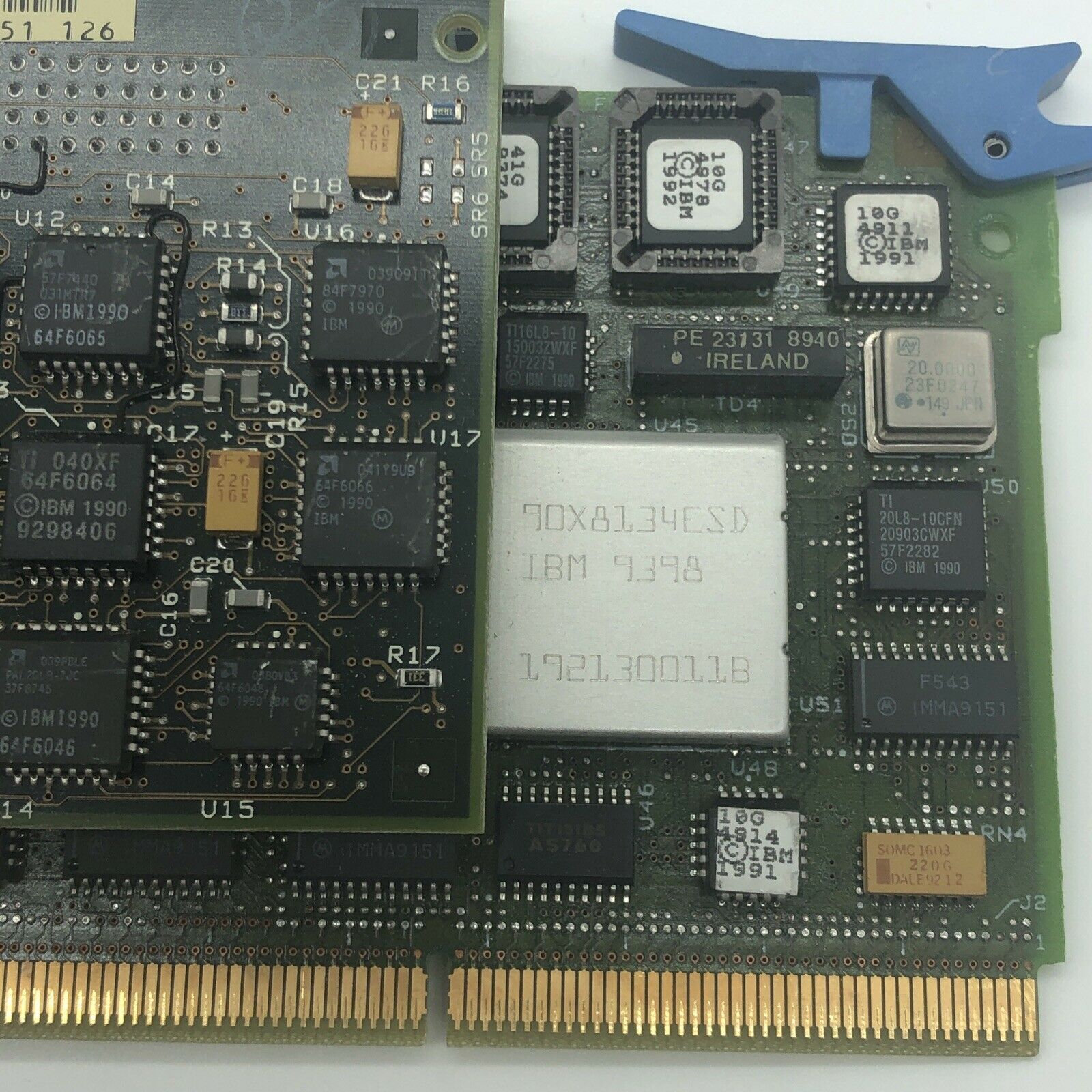
Upgrade 486DX2 66 MHz
FRU P/N 92F0145, P/N? 52G9480, FCC ID ANOIBM486B33 or ANOIBM486B66 (misprint?)
192-178 IBM PS/2 486DX2-66 PROCESSOR UPGRADE OPTION
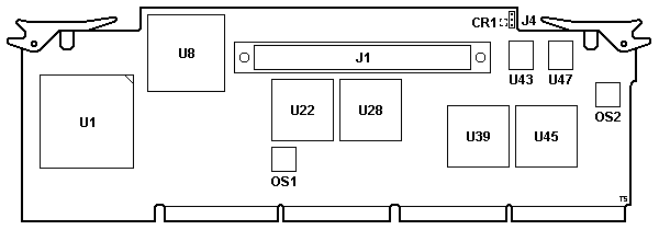
U43/47 - system firmware, 2x
Am28F010. Louis found an Upg.
486DX2-66 complex with socketed U43/47.
It's unknown whether the used devices are OTP ROMs or (Flash) EEPROMs. The
board in question is marked as FCC ID ANOIBM486B66 - an identifier not present
in the FCC database. Possibly a misprint?
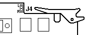
J4 Once you toggle this jumper you will
end up in a 0129 3000 error - "EEPROM Jumper is in the wrong position" and no
boot or such. I'd reported that some time ago while testing around with the
92F0145.
The jumper selects which one of the two Flash ROM devices (banks) is active
by default. The alternative setting branches into a BIOS error-code - either an
abandoned feature, or the never shipped flash updates were supposed to work
similar to the T4 platform - Stage 1 bank
altering its position with every successful BIOS update (but here without the
software-controlled bank selection to compensate for the incorrectly installed
jumper).
Note: Leave J4 jumper on the center and bottom pin
- "R".
Upgrade 486DX2 66 MHz Back
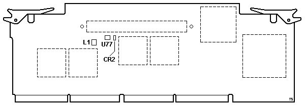
CR2 Schottky Diode B54 (Flash Vpp)
L1 Inductor 47 uH (Flash Vpp)
U77 LT1109-12 DC/DC Conv. (Flash Vpp)
U77, CR2, L1 (plus some other passives)
are part of a local 12 V voltage generator. This additional "programming
voltage" (Vpp) is required by the Flash memory to perform erase/write
operations. Its general topology closely replicates the "Flash Memory VPP
Generator" circuit from the LT1109
datasheet (page 1).
Peter says:
As a follow up notice: Yes, it *has* a Flash ROM BIOS. And, yes,
it comes up with the Type 1 reference disk. Even installs a reference partition
as usual with these disks.
But the system permanently fails to boot into this Type 1 reference
partition. Once you reboot it and press [ctrl]+[alt]+[ins] at CP 66 (cursor top
/ right) the machine loads the operating system instead jumping into
reference.
The platform nicely takes the Kingston Turbochip *without* restoration of
the system partition. Runs fine with it - right from the start.
Supports Non-IML Configurations
Dennis Smith found out that this complex can successfully boot without an
IML device at ID6. He booted a SCSI drive at ID0 WITH NO IML track. I did it
here with my upgrade DX2-66.
His guess was this complex was designed to support RAID Arrays, and the
early RAID controller, "Passplay" had no ability to boot from an array.
Upgrade 486DX 50 MHz
FRU P/N 92F0048, FCC ID ANOIBM486A50
191-096 Personal System/2 486/50 Processor Upgrade Option
52G9509 "8590/95 Dual Booting Capability EPROM" HERE
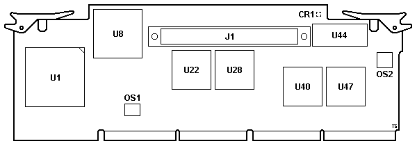
U44 Complex BIOS Stock version is
91F9812. This version does not fully support the F/W SCSI [Corvette] and IML
from up to 3.94 GB drives.
To get the most out of this complex, you need the
52G9509
"8590/95 Dual Booting Capability EPROM" -AND- the SCSI adapter needs the
92F2244 and
92F2245 SCSI BIOS Firmware.
All Spock Prime,
SCSI A/16 (short Tribble), and all
Fast/Wide SCSI adapters come stock with
the 44/45 SCSI BIOS pair.
Note: This complex needs the 15 ns cache. The
other Type 1 complexes use 17 ns memory.
Some observations:
The chipset appears the same as other Type 1s with the addition of
decoding circuitry.
The Upgrade 486DX-50 is a Type 1 with true 50 MHz CPU on
the complex! All Type 1 complexes [except "G"] use a 160 position 4x40
receptacle for the L2 Cache option. Having the 486DX-50 on the complex PCB
instead of a daughtercard means that any upgrade CPU will NOT be getting close
to a Model 90 memory riser!
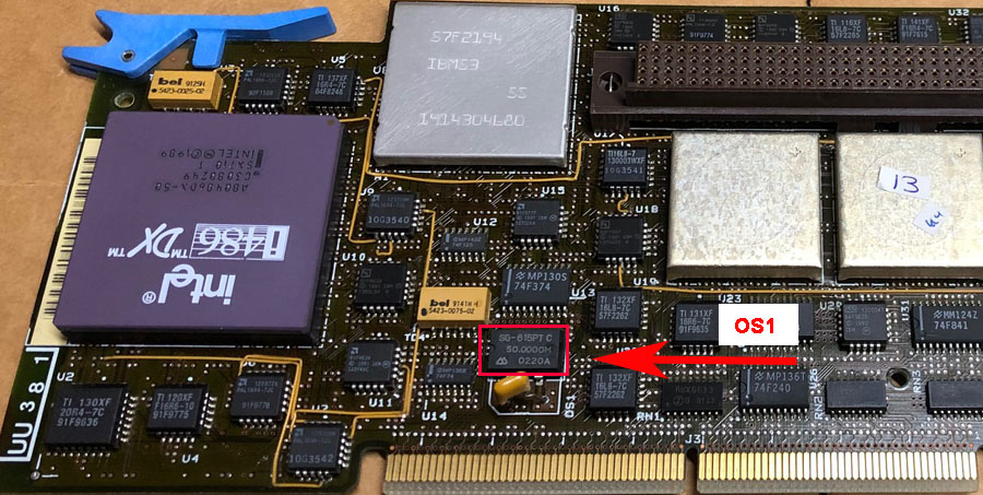
Note: On the Upgrade 486DX-50, the CPU clock,
OSC1, has been moved from being under the left side of U16. It is visible even
with an L2 Cache option installed. OSC1 is a black SMD, so if you don't see a
shiny oscillator like you are used to, look again.
Note: The Type 3 "M" complex is the only other
true 486DX-50, but the "M"'s DX-50 is on the daughtercard! (M is also called
the "double-decker")
Note: The Type 3 "M" complex is the "Enhanced
486/50" while the Type 1 486/50 is the "486/50 Processor Upgrade"
Identify Upgrade 486/50
I have noticed that sometimes, an older complex that was replaced is put
into the box from the upgrade.

To positively identify the Upgrade 486/50, look at the
back for the FCC ID sticker. It should say "FCC ID ANOIBM486A50".
What happens: A 486/33 "K" is replaced by a 486/50, the "K" is put into the
box, and through no fault (it is almost 30 years old!) the complex is called a
486/50 because that's what is on the box... This happens with other adapters as
well.
The 486/50 is easy to identify, the location of OS1 is to the left of other
Type 1 complexes, OS1 is 50.0000 MHz, and OS1 is an SMD (black plastic). All
other Type 1 complex use metal canned oscillators.
Note: The yellow component just below OS1 is "A5C
334K".
So if you want the fastest Type 1 complex, remember that Black is
Beautiful!
How is this different to the other T1 boards and the T3 Enhanced complex?
From Peter:
As far as I can tell (from the pictures of that complex) it varies
through some different wiring and modified ASICs. The part of the hardware that
deals with the CPU clock generation looks a bit different. The rest of the card
is the "later" Non-SOD Type 1 platform as I have it here in my trusty old
AKD.
It seems as if IBM wanted to offer an upgrade path to DX-50 *without* the
ECC option - for those customers that have a -xKx machine already and for the
Mod. 90 maybe, which does not cope with the "double-decker" DX-50 Type 3
platform very well. This board was not offered with any particular Mod. 90 / 95
right from the start. It has been an option only.
We, the god-Emperor:
As surmised before, the T1-50 "Big 50" was released to allow
486DX-50 power without ECC support without the need for the double-deck M. I'm
not so sure that is the case:
191-198 IBM PS/2 486SX/25,33,50 PROCESSOR UPGRADE OPTIONS Oct 17, 1991
192-101 IBM PS/2 ENHANCED 486/50 PROCESSOR UPGRADE OPTION Apr 28, 1992
To be clear about the improvements in the M complex:
Enhanced dual path memory design (Dual Bus Interleave). Although
Base 1 allows both the processor and busmasters to access memory concurrently
through two paths, the Base 3 and 4 has buffers at both paths to provide better
performance. Also the buffer on the adapter side (I/O buffer) uses packet data
transfers for writes. This means 16 bytes are collected and this packet is
written in one cycle to memory as opposed to writing for every 4 bytes received
(as with unbuffered systems).
Tom sums things up:
The T1 Upgrade 50 board is (obviously) just an incremental
improvement of the existing T1 design. It provides higher CPU performance, and
comes standard with L2 cache. But that's about it... Other than that, it's just
the same "old" T1. The R&D time and costs would be relatively low with this
one, so IBM would be able to push it out to the market quicker and for more
accessible price (in IBM terms...).
The Enhanced T3 50 complex, on the other hand, is a drastically different
beast. It brings not only a higher CPU performance, but also better system
throughput, thanks to its improved design and streaming capabilities. It also
comes with a 32-bit DMA controller, ECC memory support, and more. All these
enhancements were of course reflected by its development time and price
tag.
So, clearly what we have here are two very different designs, with different
capabilities, release dates, and price points. If your server needed some more
CPU headroom and it needed it now (late 91/early 92), the T1 Upgrade 50 would
have been the right choice for you. If you sought after higher overall
performance, or some of the new features, the Enhanced T3 platform would give
you that. For extra $$$...
Lorenzo Mollicone:
The Announcement Letter says "... an external 256KB level two
cache is provided as standard on the processor complex" All of my boxed Upgrade
486DX-50 Processor Upgrade Options have the L2 Cache.
256 KB Cache Memory Option Kit
17 ns and 15 ns
Note: In a advertising/tech nugget booklet, IBM
ran tests with a number of (then) current applications, and the best they could
do was 6%; that is, six percent. I bet they wanted much better.
17 ns for "J" [25], "K" [33] and Upgrade 486DX2-66 [33] complexes
15 ns for Upgrade 486DX-50 [50] MHz complex
The 256 KB cache is a 5.5 x 3.0 inch card that connects to either the 25, 33
or 50 MHz complex. The connector is 160 pins arranged in four columns and 40
rows. The complex provides all the power required to drive the 256 KB
cache.
256 KB cache memory option three basic logic elements:
- 256 KB of SRAM
- 4 KB of TAG SRAM
- Cache Controller
256 KB of Static Random Access Memory ("Data SRAM"). This is two-way set
associative, which allows each index location in the cache to store two pieces
of information. This improves the hit ratio, and decreases the number of times
that cache items must be removed to make room for new items.
4 KB of "TAG SRAM" stores some of the cache item's address bits, used to
store and locate the item, and some bits used for validity checking.
"Cache Controller" coordinates access to the SRAM. On a cache-hit, the
controller organizes the access of the data from the data SRAM using the TAG
SRAM address. On a cache-miss, the controller places the new data into the
cache, updating the TAG SRAM and data SRAM at the correct index location.
The controller is also responsible for ensuring that the address being
searched for is actually a cacheable address. If not, no cache search will be
done.
The L2 cache is controlled through the Cache Control Register (E2h), and its
status is indicated in the Cache Status Register (E3h).
Optional Cache Card Installation
Plug the 256 KB cache onto the receptacle on the complex. One pin, called
the "key", has been removed to provide a guide for inserting the card
correctly.
256K Cache Not Visible under System programs?
After installing the 256 KB cache, the processor will simply begin to use
the cache. It will not appear in the configuration of the system. The only time
you will see the L2 Cache in a message is when it is malfunctioning.
256K 17 ns Cache Daughtercard P/N 6451095 or 64F0199
The PS/55 Type 1 complex uses a different 17 ns cache module (79F1293).
64F0199 Front
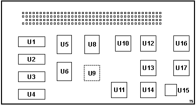
U1-4 TC55329J-17 32Kx9 SRAM
U5,6,8 SN74ACT2160-17FM 8Kx4 TAG
U10 64F6043 PAL
U11 84F8257 PAL
U12 64F6065 PAL
|
U13 84F8261 PAL
U14 64F6046 PAL
U15 64F6048 PAL
U16 84F7970 PAL
U17 64F6066 PAL
|
U5,6,8 SN74ACT2160-17FM
8Kx4 2-Way Cache Address Comparator/Data RAM
(databook pp 170)
Note: The chips change from module to module.
Yours may be different. The cache controller is implemented using PAL/GALs (AMD
chips).
64F0199 Back
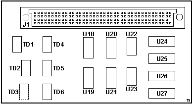
J1 159-pin connector AMP 650754-1
TD1 Fil-Mag 77Z14A030 30 ns delay line
TD2,4 Fil-Mag 77Z14A025 25 ns delay line
TD5,6 Fil-Mag 77Z14A045 45 ns delay line
|
U18-21 IDT 74FCT646ASO
U22,23 74AS573
U24-27 Toshiba TC55329J-17
|
U18-21 IDT 74FCT646ASO
Fast CMOS Octal Transceiver/Register
(databook pp 417-422)
TD?
Fil-Mag or Sprague 77Z14Annn Active TTL Delay Module
Equivalent to bel S423-00nn Active TTL Delay Module
256K 15 ns Cache Daughtercard P/N 92F0050 or 10G3527
92F0050 Front
(thx to Lorenzo Mollicone)
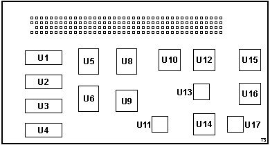
U1-4 MCM6205NJ15 32Kx9 SRAM
U5,6,8 SN74ACT2160-17FM 8Kx4 TAG RAM
U9 91F9757? PAL
U10 91F9775? PAL
U11 10G3532 PAL
U12 91F9783 PAL
|
U13 ? PAL
U14 91F9780 PAL
U15 91F9785 PAL
U16 91F9784 PAL
U17 91F9781 PAL
|
92F0050 Back
(thx to Lorenzo Mollicone)
U18 MC88915FN55 Low Skew CMOS PLL Clock Driver 55 MHz
Significant change from 17 ns version. The 64F0199 uses five Delay Modules
and the 15 ns uses just one.
How Does System Know That L2 Cache is Installed?
Some of the pins on the L2 connector are most likely used as "presence
detect" lines (i.e. floating high by default and tied low when the module is
installed). This allows the firmware and system configuration/diagnostics
software to detect the cache module and possibly to distinguish between the
different types as well. The state of these lines can be read back through I/O
port E2h - "Cache Status Register" (bits 4 and 5).
The complex/daughtercard doesn't have a POS ID (only the planar and adapters
have one), so the US5530887A patent
doesn't apply here.
L2 Cache Performance
From Us, the god-Emperor of Microchannel:
Praytell, what use can one make of the 256K cache for the T1
complexes? I hate to admit it, but I never noticed a large (or significant)
boost when I added one.
From Tony Ingenoso:
The effects of modern bloatware on a write-through can be
disheartening... IMO IBM's matched cycle scheme goes a long way towards helping
keep the L1 lines filled at a brisk pace even when no L2 is present. The T2's
abnormally good performance (considering its other genetic limitations) shows
this well. For all practical purposes, 90/95's have a 64 bit memory subsystem
working to fill the L1 lines.
From Charles Lasitter:
What do you see with one speed processors (DX50) that are coupled
with a faster cache 64F0050, or the T3 and integrated cache? Since they don't
have a 'fall back' processing speed in the event of an L1 miss, but rather use
a 15 ns L2 vs 17 ns, is there any difference for them?
I believe we've seen LARGE increases in speed when doing something
like kernel rebuilds compared to no cache. I think it may depend on what you're
doing and the operating system.
From Tony:
I don't see this as a core multiplier issue -- even the low end
DX25 T2 runs better than one might expect it to. The kernel rebuild
improvements aren't surprising - compilation algorithms and the bits of data
they work tend to be well localized if modules aren't too massive. Initial
parsing would be very read intensive as well and should make good use of an L2.
Cache performance is indeed a very task specific kind of thing. Scattered
code/data can effectively neutralize it totally.
DX50's are strange -- they often outrun DX2-66 when main memory bandwidth or
I/O is the constraint. When staying in L1, then the DX2-66 wins due to the
multiplier. With a fast L2 and fairly scattered code/data a DX50 is going to do
very well.
From Peter:
Uhmmm... I had the occasion to test a T1 DX2-33/66 board under
Linux. And compare it with the same T1 DX-50 (!) board - both with the L2
cache.
The 486DX2-33/66 showed 33 BogoMips, the DX50 25 only... same as the T3 DX50
while a DX2-50/100 (Intel DX4-100 in 2x mode) on a T3-platform runs at
-supposed- 50 Bogomips almost.
In the practical use the T1 DX50 wasn't much slower than the T1 DX2 - the
XF86 stuff paced at the same rate on both. None of the machines "felt" faster
or slower. The DX4 T3 was a bit faster - but not significantly. All 3 machines
had the same XGA-2 card, the same TR 16/4 network adapter, the same 32MB Parity
RAM and the same IBM 400MB HD with the Linux on it.
The T1 platforms had the "plug on" 256K L2 cache (17 ns on DX2, 15 ns on
DX50) and the T3 had its own integrated cache. I did not write down all the
values... maybe I should repeat that session again to get some definite,
comparable data.
ODP vs. ODPR
169-pin ODP - 487SX installed with 486SX still in place, needs the
"SX-disable" pin. Important on boards with soldered CPU.
168-pin ODPR - (R - "Replace") replaces 486SX / 486DX does not need "SX-disable" pin.
System Firmware (POST & BIOS)
Simplified firmware stored in EPROM (except for the Upg-66
complex that uses Flash memory). IML image required for the system to operate.
ROM Images
All ROMs are 27C010 or compatible (position U36 or U44).
64F4474 - 24 Apr 1990, rev. 0, Type 1 "J" with Weitek socket
84F9154 - 18 Jun 1990, rev. 0, Type 1 with Weitek socket or "SOD" solder pads
84F9155 - Unknown date and rev., Type 1 "J" or "K" with Weitek socket
91F9812 - 09 Jan 1991, rev. 1, Type 1 without Weitek socket, non-SOD
52G9509 - 03 Mar 1992, rev. 3, "Dual Booting Capability EPROM"
Support for >1 GB Disks as IML Drive
Type 1 complexes require the combination of
BIOS 52G9509 and SCSI
BIOS 92F2244/45 in order to handle IML drives >1GB (new limit is 3.94GB).
The upgrade BIOS incorporates the "Enhanced IML" which supports IML from a
drive >1GB and "Search IML" which allows IML from a drive other than ID6.
The SCSI BIOS 44/45 pair supports drives well over 8GB. (Ed. You OS may have
other ideas...)
More information HERE.
Some Other Thoughts
From Charles Lasitter:
I've had some VERY entertaining results in my installations,
depending on what other drives were present, and which version of the processor
BIOS was used.
With the 52G9509 in place, ID6 in bottom bay (Mod 95) at end of cable, ID5
in bay above on next spot on cable, I couldn't get the IML to go to ID6 to save
my ass. It made a beeline for ID5 every time. Put in the old BIOS, and it goes
straight for ID6.
Enhanced BIOS Effects
From Charles Lasitter:
As a result of a programming project with Mr. Clarke, I am now
fairly certain that the odd behavior of an IBM SCSI controller "ignoring" ID6
to lay an IML track on a drive that was ID5 was really a function of the
enhanced BIOS, which sniffs out the signature of any current or previous IML
partition on a series of drives, and insists upon installing or recovering a
system partition to that same location.
This same feature is related to the IBM controller's inability to do an
actual format of the drive if there has been an IML partition on the drive
before. The space at the end of the drive is never released, because the IBM
controller refuses for format that area of the drive.
That's why I typically use the RAID adapter when I REALLY want to nuke some
drives.
Upgrade EPROM Additional Capabilities
- More efficient use of Adapter ROM memory minimizes adapter configuration
conflicts.
- BIOS support for IML drives up to 3.94 gigabytes per device.
- Supports "Search IML" from any PUN or SCSI ID. System partition is no
longer restricted to SCSI ID=6. Each HD ID is searched for valid system
partition.
- Allows redundant system partitions (IML).
- Sharing of SCSI devices. An external SCSI device, (ex. 3511), may be shared
between two system units.
Type 1 complexes (except DX2-66 Upgrade, 92F0145) need BIOS 52G9509 to
handle IML drives of >1,023MB. (U36 in drawing)
Complex EPROM Speeds
Most T1 complex boards come with a 120 or 150 ns EPROM, but the actual ROM
read cycle is going to be even slower than that. So, since the timing is fixed
(forced wait-states), replacing the ROM with a faster chip will not affect
how long the Stage 1 POST takes to execute. Using a significantly slower EPROM
may however cause trouble (read errors).
The Stage 2 POST code is loaded from the IML drive to RAM, verified, and
then executed for RAM. The hard-drive speed is pretty much irrelevant here
since the entire IML image is loaded at once and is only 128 KB in size.
Am27C010 versus Am28F010
I was diddling about, looking to turn out some 52G5909 T1 Upgrade BIOS for
Lorenzo. In my desire to be lazy, I thought getting some EEPROMs would make my
life easier, no UV eraser needed, just "Blank Device". So I pumped out five
28F010, and it is great! Blank 'em and program, no UV eraser needed... and then
I ran into "Stuck bit Hell". I struggled through 20 28F010 in order to get ten
good EEPROMs. I then sent my love children to Lorenzo, thinking, "Hey, they
verified and have the same checksum, must be good". But I was wrong.
Lorenzo said:
Swapped BIOS chip, video never goes live. Tried two chips, both
don't seem to initialize.
So, experience suggests that you stay with the same device family or
hilarity may ensue... I can't explain in detail why, but I sure as heck can say
it didn't work for me. YMMD
Ed. The pinouts are compatible (the only
difference is pin 31 - marked as PGM# in case of Am27C010 and as WE# for Am27F010).
Ed. Tom: When programming flash chips it's
important to select not only the correct family but also the correct
manufacturer and the exact device type.
Type 1 Complex Upgrade to "8590/95
Dual Booting Capability EPROM"
Complexes with the following EPROM part numbers
may be upgraded:
| Processor |
FRU P/N |
Model |
EPROM P/N |
Loc. |
| 20 MHz SX |
92F0049 |
0Gx |
91F9812 |
U36 |
| 25 MHz DX |
64F0201 |
0Jx |
84F9154 or 91F9812 |
U36 |
| 33 MHz DX |
64F0198 |
0Kx |
84F9154 or 91F9812 |
U36 |
| 50 MHz DX |
92F0048 |
P3 (UPGD) |
91F9812 |
U44 |
It was called the "8590/95 Dual Booting Capability EPROM Package".
Part number 52G9509 (was 52G9750 - try this if other P/N is not known)
Note: Use the latest refdisk and diags. See
above...
Data Buffers
(source)
The T1 processor complex has three data buffers. Two of these are connected
to the two memory banks on the planar, and one is connected to the Micro
Channel bus.
The main purpose of these buffers is to ensure that the processor receives
its data on the correct lines. For example, the processor expects 32 bits of
data. If a device on the Micro Channel sends 8 bits, the data buffer will make
sure the bits arrive on the data lines that the processor will be
expecting.
The data buffers attached to the planar memory have an additional function.
They allow 64 bits of data to be held at a time. This allows the processor to
access the first 32 bits of data, and then very quickly access the second 32
bits, without refilling the buffers. This ability speeds up access to memory,
and improves system performance.
The MCA and memory buffers are implemented using the same type of device.
There are however two different part numbers are associated with the Data
Buffer ASIC - 54F2958 (older?) and 78F1659 (newer?). It's currently unknown
what the difference is between the two (if any).
CR1 Diagnostic LED (unpopulated)
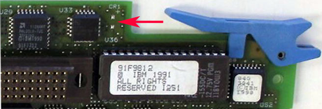
You can see this on a number of Type 1 complexes, including the Upgrade
486DX2-66 and the Upgrade 486DX-50. What is CR1 for?
Lorenzo populated the position with a LED and:
No blinks, no on-off. Solid glow.
Tom says:
Judging by its convenient location right in the corner, it was
probably supposed to be a diagnostic LED.
Tom later on:
Turns out that you can control the LED (if you populate it first)
by toggling bit 1 of port E2h (0: LED off, 1: LED on). I don't think the bit
controls anything else on the complex. Pretty sure it's just a debug LED,
similar to CR1/2 on the T4 platform. It was
probably used during the development, and then dropped from the production
boards. The shipped firmware doesn't use it in any way it seems.
| 