|
rf7080a.exe Model 70/80 386 Reference Disk v1.12 (zipped image)
Warning: The original Micral 500 refdisk
is pure unobtainium. Use the PS/2 Model 70/80 refdisk to configure the system.
It's not perfect (base memory not being reported correctly) but it works.
Paradise/WD VGA files (Metropoli BBS files, archived)
Specifications
Micral 500 Planar
Chipset
System Firmware
ROM Images
Exhaust Fan Assembly
Speaker/Battery/LED Assembly
Interconnect Board
LED Board
Battery Pack
Speaker
Power Supply
Photos, ROM images, and other material provided by Stefan Lemanski.
Specifications (Type CPU1334)
![[P]](/other/img/photo.gif "Top (open)")
CPU: i80386DX 20 MHz (PGA), optional math co-pro (PGA)
Memory: 8x 30-pin SIMM slot on the planar (industry standard?)
Bus: MCA, 1x 32-bit, 3x 16-bit (one w/ AVE, one internal)
Video: Paradise VGA (on-board), 256 KB video RAM
HDD: WD1007V-MC1 ESDI + Seagate ST1201E (200 MB)
FDD: 3.5" 1.44 MB (34-pin, Mitsubishi MF355C-213U)
I/O: PS/2 keyboard & mouse, 1x 25-pin serial, 1x parallel
The machine imitates the original PS/2 Model 80 with the 16 MHz Type 1 planar
(ID FEFF, model F8, submodel 0).
Micral 500 Planar N290619000-08K, A-M-020078
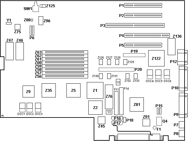
F1 125 V / 3 A LF Fuse (PS/2?)
OSC1 48.0000 MHz osc
OSC2 40.0000 MHz osc
OSC3 14.3181 MHz osc
OSC4 36.0000 MHz osc (PVGA mem.)
OSC5 28.3220 MHz osc (PVGA video)
OSC6 25.1750 MHz osc (PVGA video)
P1,2 16-bit MCA slot
P3 32-bit MCA slot
P4 16-bit MCA slot w/ AVE
P5 Internal 16-bit MCA slot (ESDI ctrl.)
P6 Speaker/battery/LED connector
P7 Mouse port
P8 Keyboard port
P9 Parallel port
P10 DB25 serial port
P11 34-pin floppy connector
P12 HDD15 video connector
P14 40-pin IBM floppy connector?
P15 Exhaust fan connector
P16 Molex power connector (HDD)
P17 Pads for Molex connector (HDD)
P18 Berg power connector (FDD)
P19 Pads for 2x18-pin connector
|
P20 Pads for video RAM socket?
SW1 Pads for a switch (reset?)
Y1 32.768 kHz? xtal (RTC)
Y2 10.000 MHz xtal
Y3 16.000 MHz xtal
Z1 PGA-132 socket w/ i80386DX-20
Z2 PGA-68 socket for math co-pro
Z5 G2 GC183 DMA ctrl.
Z9 G2 GC181 CPU/Bus ctrl.
Z35 G2 GC182 Memory ctrl.
Z45 WDC WD57C65JM FDC
Z46 BIOS ROM Even "S/802-06"
Z47 BIOS ROM Odd "S/803-06"
Z56-63 30-pin SIMM sockets
Z75 Motorola MC146818A RTC/CMOS
Z76 D8742 K/B ctrl. "S/804-02"
Z81 G2 GC186-PC PIO ctrl.
Z88 TI TL072C op-amp (PC speaker)
Z91 NS16550AFV UART
Z96 CXK5864BM-10L 8Kx8 SRAM (NVRAM)
Z122 Paradise PVGA1A (alt)
Z125 3 DIP switches (+pads for 2 more)
Z126-133 KM41464AJ-12 64Kx4 (VGA)
Z136 inmos IMSG171P-35C RAMDAC
|
P17 The second Molex connector is not
populated and the +12 V pad is jumped by a thick bodge wire directly to the PSU
edge connector. The original +12 V trace was probably too thin to satisfy the
HDD/FDD current draw.
Z2 There's a small PCB under the math
co-pro socket. It only contains a resistor network and two discrete resistors.
(pullups or termination?)
P5 Internal 16-bit MCA slot. Comes with
the WD1007V-MC1 ESDI controller
pre-installed.
The rest of the board is covered with 74xx glue, a couple PLDs, and a bunch
of passives.
Chipset
Developed by G-2 Inc., also sold as Headland GCK181.
Headland GCK181 Universal PS/2 Chip Set Datasheet
GC181 - Bus Controller (page 3 physical)
GC182 - Memory Controller (page 15 physical)
GC183 - DMA Controller (page 27 physical)
GC186 - Peripheral Controller (page 49 physical)
Semiconductor User Information Service Newsletters 1988-1989 (page 144 physical) says:
"LSI Logic's affiliate, G-2, has entered into an agreement with
Groupe Bull of France to manufacture an IBM PS/2 compatible chip set. The chip
set includes the GC181 CPU bus controller, the GC182 memory controller, the
GC183 DMA controller, the GC184 address-data buffer, and the GC186 peripheral
controller. The 20-MHz chip set, which will be sampled in the third quarter of
1988, will be fabricated with a 1.5-micron (1.2-micron effective) CMOS process.
(25 Jul 1988)"
System Firmware (POST & BIOS)
Firmware stored in EPROM.
ROM Images
All ROMs are AMD Am27C512-155DC, positions Z46/Z47 (even/odd).
S_802-06 / S_803-06 - BULL SYSTEM BIOS Version B1.1a (rev. 5, 09 Nov 1989)
Exhaust Fan Assembly
The construction of the fan assembly is similar to that of the Model 50.
Plastic shroud with a fan and small PCB inside. The fan is held in place with a
foam, no clips, no screws...
Fan Model
SANYO
BRUSHLESS DC Mini Ace 25
MODEL 109P0912M4021
DC 12 V 0.1 A
SANYO DENKI CO.,LTD.
MADE IN JAPAN
Dimensions: 92mm, 25mm thick
SAN ACE 92mm MINI ACE DC Fan Motors Datasheet
Fan PCB "VENTIL." 729059008-00A
The fan PCB has a provision for two passive components (resistor + thermistor?)
but neither was populated on the only sample we have seen (possibly a crude
temp control?).
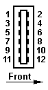
Fan Connector Pinout
6-pin card-edge connector on the planar board.

|
| Pin | Signal | Pin | Signal |
|---|
| 1 | Ground | 2 | N/C |
| 3 | +12 V | 4 | N/C |
| 5 | +12 V | 6 | N/C |
|
Speaker/Battery/LED Assembly
The assembly consists of the support frame, an interconnect PCB, an LED PCB, a speaker, and a battery.
The frame also doubles as an adapter card support.
Interconnect Board "C. INTERCONNEXION" 7290582008-01C
Edge Connector
12-pin card-edge connector on the planar board.
|
| Pin | Signal | Pin | Signal |
|---|
| 1 | N/C | 2 | Speaker Data |
| 3 | N/C | 4 | GND (Spkr./Batt.) (?) |
| 5 | "ST" Jumper (?) | 6 | Battery+ |
| 7 | Hard-Drive LED- | 8 | Hard-Drive LED+ |
| 9 | Power LED- | 10 | Power LED+ |
| 11 | N/C | 12 | N/C |
|
P2 "LED" - LED Board Connector
| Pin | Signal |
|---|
| 1 | N/C |
| 2 | Hard-Drive LED+ |
| 3 | Hard-Drive LED- |
| 4 | Power LED+ |
| 5 | Power LED- |
| 6 | N/C |
P3 "H.P." - Speaker Connector
| Pin | Signal |
|---|
| 1 | Ground |
| 2 | Speaker Data |
P4 "BAT" - Battery Connector
| Pin | Signal |
|---|
| 1 | Physical Key |
| 2 | Battery+ |
| 3 | Physical Key |
| 4 | Ground |
"ST" Jumper
Clear CMOS jumper?
LED Board "CARTE LEDS" 7290589008-00A
Contains the Power ("A/M") and Hard-Drive activity ("DISQUE") LEDs.
Plugs into the Interconnect Board.
Battery Pack
The battery pack consists of two Li-Ion 2.5 V non-rechargeable AA cells
wired in series to give approx. 5 V total. The cells are stuffed in a box
with a 4-pin header connector attached to it via a twisted pair wire.
The pack is wired to the Interconnect Board.
You probably won't be able to get a replacement battery pack, but you can
open the original one and replace the cells. Alternatively, you can replace the
entire thing with a battery holder or another battery with equivalent specs.
Warning: Never solder directly to a battery/cell.
Either buy cells with contacts already attached, get a mini spot-welder, or use
a battery holder. Excessive heat may damage the cell and lead to a fire or an
explosion! You are doing this at your own risk.
Original Battery
Made by SAFT
Lithium, 5.2 V, 2.3 Ah
BULL 76957876 002
Speaker
Bukooo
66SP03
8 Ω 0.4 W
Plugs into the Interconnect Board.
Power Supply
Similar form factor as the Model 50/70 PSU,
but bigger.
ASTEC Model No. BM135-3301
Input: 230 V AC, 1.8 A, 50/60 Hz
Output voltages:
| Voltage (DC) | Pin # | Current / Pin |
|---|
| -12 V | 1 | 500 mA |
| +12 V | 3,5,7,9,11,13 | 667 mA |
| +5 V | 15-47 odd # only | 940 mA |
| DC Return | 2-48 even # only | 1000 mA max. |
| Power Good | 50 | — |
Maximum continuous output power is 135 W.
The pinout is the same as for the
Model 50/70 PSU, except for the
"System Status" signal on pin 49 that is missing here (hard-drive activity LED
on Models 50/70).
|