|
Pinout Comparison with 72-pin SIMMs (from Peter)
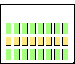
Planar Memory Cards
Planar Memory Sizes
System Support of Planar Memory Sizes
Memory Card Connector
Planar Memory Pinout
Presence Detection
Planar Memory Cards (thx to David Beem for the ref. photos)
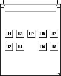
IBM 1 MB Memory Card
P/N 15F6821, 4098553*
![[P]](/other/img/photo.gif "Front") |
|
|
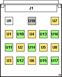
J1? Planar connector
U1-9 89X8921(ESD) or 6470780(ESD)* 1Mbit DRAM?
(no components on the solder side)
|
IBM 1 MB Memory Card
P/N 15F6820, 4098539(A)*
|
|
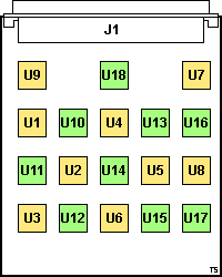
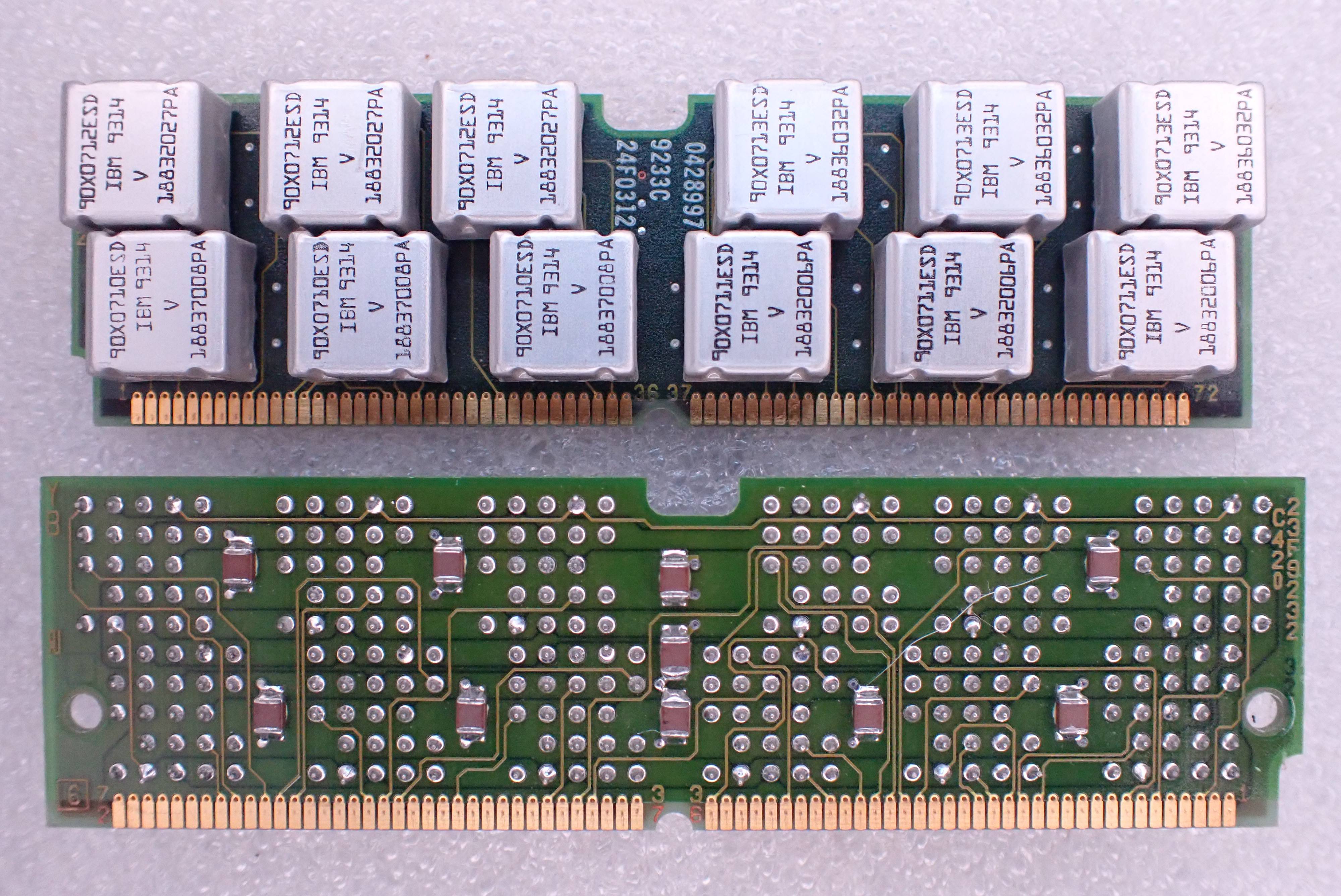
IBM 1 MB Memory Card
P/N 72X7475(A), 90X9438
|
|
|
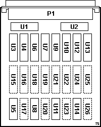
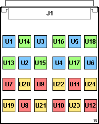
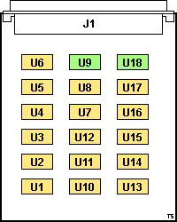
J1 Planar connector
U1-9 90X0706(ESD) or 89X9822(ESD) or 89X9430(ESD)? ![[yellow]](/other/img/l_yellow.gif "Yellow")
U10-18 90X0705(ESD) or 89X9821(ESD) or 89X9429(ESD)? ![[green]](/other/img/l_green.gif "Green")
(no components on the solder side)
|
IBM 1 MB Memory Card
P/N 15F6773
IBM 2 MB Memory Card
FRU P/N 92F0669, P/N 92F0664
/ FRU P/N 90X7391, P/N 15F6824
IBM 2 MB Memory Card
P/N 90X8670
(src) |
(src) |
(src)
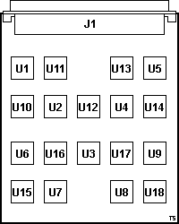
|
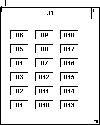
J1 Planar connector
U1-18 6470780(ESD)? 1Mbit DRAM?
(no components on the solder side)
|
IBM 2 MB Memory Card
FRU P/N 90X7391, P/N 90X9019
/ P/N 90X8993
(src)
/ P/N 15F6823(F)*
IBM 2 MB Memory Card
FRU P/N 92F0669, P/N 92F0662
/ P/N 15F6822
IBM 2 MB Memory Card
FRU P/N 90X7391, P/N 15F6825
|
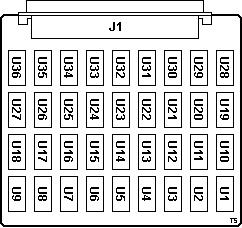
IBM 4 MB Memory Card
FRU P/N 34F0023 or 33F5538*, P/N 33F5498
|
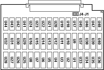
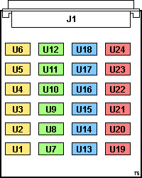
J1 Planar connector
U1-36 89X8922 or 23F7261 or 23F7233*
(only bypass caps on the solder side)
Marked as "4MB SYSTEM BOARD MEMORY III" on the PCB.
Based on the silkscreen format and IC plant code 93 this card was most likely
designed and manufactured by IBM Japan.
|
Kingston KTM-1000/M80 1 MB Memory Card (REV._)
|
|
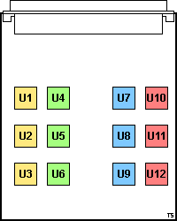
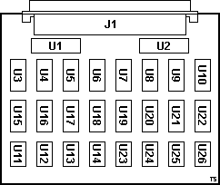
P1 Planar connector
U1,2 Am2966PC octal DRAM driver
U3,4,6,7,9,10,12,13 KM44C256AP-8 256Kx4 DRAM
U5,8,11,14 KM41C256P-8 256Kx1 DRAM (parity)
U15,16,18,19,21,22,24,25 Pads for KM44C256AP-8 256Kx4 DRAM
U17,20,23,26 Pads for KM41C256P-8 256Kx1 DRAM (parity)
Empty positions for additional 1 MB of DRAM for 2 MB total.
All through-hole parts.
(no components on the solder side)
|
Kingston KTM-2000/M80 2 MB Memory Card (REV.A00)

|
P1 Planar connector
U1,2 Am2966PC octal DRAM driver
U3,4,6,7,9,10,12,13 KM44C256AP-8 256Kx4 DRAM (low MB)
U5,8,11,14 KM41C256P-8 256Kx1 DRAM (low MB parity)
U15,16,18,19,21,22,24,25 KM44C256AP-8 256Kx4 DRAM (high MB)
U17,20,23,26 KM41C256P-8 256Kx1 DRAM (high MB parity)
All through-hole parts.
(no components on the solder side)
|
Kingston KTM-4000/M80 4 MB Memory Card (REV.A00)
Unidentified 4 MB Memory Card
Cumulus CuMEM 80/4
P/N 8020238
|
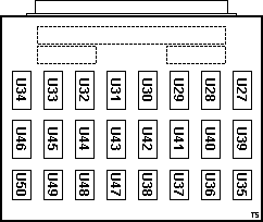
J1-4 Pads for jumpers - J2 and J4 shorted (presence detect?)
U1-16,25-40 MSM514256A-80R 256Kx4 DRAM
U17-24,41-48 P21256-08 256Kx1 DRAM
All through-hole parts.
(no components on the solder side)
|
Planar Memory Sizes
System Board 16 MHz (8580-041, 071) 33F8416
1 MB 80 ns Memory Kit (for 33F8416) 72X6670 or 6450375
72X7475 found
System Board 20 MHz 10G4148 (8580-081, 111, 121, 161, 311, 321)
2 MB 80 ns Memory Kit (for 92F0756) 92F0669 or 6450379
92F0669 found. 90X7391 in Jan 1992 Pocket Ref Manual.
System Board 25 MHz 85F0046 (8580-A21, A31, A61)
4 MB 80 ns Memory Kit (for 85F0046) 92F0106 or 6451060
33F5498? 34F0023 in Jan 1992 Pocket Ref Manual.
System Support of Planar Memory Sizes
(by Fred Spencer, original HERE)
On the initial 8580 models, only 1 MB and 2 MB planar memory modules were
available. With the announcement of the 25 MHz
planars (8580-Axx), 4 MB memory cards became available. However, it has
been discovered that they will function on the 20 MHz planars (thanks to Tim
Clarke and Joe Kovacs for this discovery). A summary table of my experiences
using various sizes of memory cards in each of the three categories of planars
follows:
Memory
Card Size | Planar Type |
|---|
| 16 MHz | 20 MHz | 25 MHz |
|---|
| 1 MB | OK | OK | ER. 225 |
| 2 MB | OK | OK | ER. 225 |
| 4 MB | 2 MB | OK | OK |
Note 1: 16 MB planar can use 4 MB card, but can
only use 2 MB. [ed.]
Note 2: ER. 225 is the POST Error Code resulting
from having memory that is too slow.
Note 3: On some 20 MHz planars with 4 MB memory
cards on the planar, the IBM diagnostics will occasionally fail, but the memory
will still function OK. With the PIICEON 4 MB (70 ns) memory card the IBM
diagnostics may also fail. However, both the IBM and PIICEON 4 MB memory cards
will function properly and they do pass the Norton Utilities memory diagnostics
without any problems. I will be doing more investigation regarding this.
Memory Card Connector
DIN 41612 Type R - 96-contact inverse female three row connector (90° pin termination)
Burndy RPI96U30RB-1 or RPI96U30RB1
Panduit 130-096-553
Hi-Con Type-R Series 130
Hi-Con Overview Chart
Planar Memory Pinout
The Type 1, 2, and 3 system boards are equipped with two 3- by 32-pin system
board memory connectors. A memory card must be installed in connector 1 before
additional memory can be used in the channel.
The following figure shows the pin locations of the 3- by 32-pin system
board memory connectors. The pin locations are the same for connectors 1 and 2.
Connector 1 is closest to the power supply. Pin 32 is closest to the rear of
the system board.
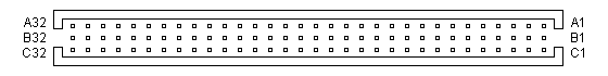
| Row A | | Row B | | Row C |
|---|
| Pin | I/O | Signal | Pin | I/O | Signal | Pin | I/O | Signal |
|---|
| A1 | N/A | Reserved | B1 | N/A | Ground | C1 | I/O | MD0 |
| A2 | I | -MW | B2 | N/A | +5 Vdc | C2 | I/O | MD1 |
| A3 | I | MA0 | B3 | N/A | Ground | C3 | I/O | MD2 |
| A4 | I | MA1 | B4 | N/A | +5 Vdc | C4 | I/O | MD3 |
| A5 | I | MA2 | B5 | N/A | Ground | C5 | I/O | MD4 |
| A6 | I | MA3 | B6 | N/A | +5 Vdc | C6 | I/O | MD5 |
| A7 | I | MA4 | B7 | N/A | Ground | C7 | I/O | MD6 |
| A5 | I | MA5 | B8 | N/A | +5 Vdc | C8 | I/O | MD7 |
| A9 | I | MA6 | B9 | N/A | Ground | C9 | I/O | MD8 |
| A10 | I | MA7 | B10 | N/A | +5 Vdc | C10 | I/O | MD9 |
| A11 | I | MA8 | B11 | N/A | Ground | C11 | I/O | MD10 |
| A12 | I | -RAS0 | B12 | N/A | +5 Vdc | C12 | I/O | MD11 |
| A13 | I | -RAS1 | B13 | N/A | Ground | C13 | I/O | MD12 |
| A14 | I | -RAS2 | B14 | N/A | +5 Vdc | C14 | I/O | MD13 |
| A15 | I | -RAS3 | B15 | N/A | Ground | C15 | I/O | MD14 |
| A16 | O | -RAMHS* | B16 | N/A | +5 Vdc | C16 | I/O | MD15 |
| A17 | O | R | B17 | N/A | Ground | C17 | I/O | MD16 |
| A18 | O | T2* | B18 | N/A | +5 Vdc | C18 | I/O | MD17 |
| A19 | I | -CAS0 | B19 | N/A | Ground | C19 | I/O | MD18 |
| A20 | I | -CAS1 | B20 | N/A | +5 Vdc | C20 | I/O | MD19 |
| A21 | I | -CAS2 | B21 | N/A | Ground | C21 | I/O | MD20 |
| A22 | I | -CAS3 | B22 | N/A | +5 Vdc | C22 | I/O | MD21 |
| A23 | I/O | MDP0 | B23 | N/A | Ground | C23 | I/O | MD22 |
| A24 | I/O | MDP1 | B24 | N/A | +5 Vdc | C24 | I/O | MD23 |
| A25 | I/O | MDP2 | B25 | N/A | Ground | C25 | I/O | MD24 |
| A26 | I/O | MDP3 | B26 | N/A | +5 Vdc | C26 | I/O | MD25 |
| A27 | I | -BE0 | B27 | N/A | Ground | C27 | I/O | MD26 |
| A28 | I | -BE1 | B28 | N/A | +5 Vdc | C28 | I/O | MD27 |
| A29 | I | -BE2 | B29 | N/A | Ground | C29 | I/O | MD28 |
| A30 | I | -BE3 | B30 | N/A | +5 Vdc | C30 | I/O | MD29 |
| A31 | I | -CASP | B31 | N/A | Ground | C31 | I/O | MD30 |
| A32 | O | T1 | B32 | N/A | +5 Vdc | C32 | I/O | MD31 |
Note:
* Type 3 only, Reserved on Types 1 and 2
-MW: -Memory Write
-MA(0 - 8): -Memory Address (0 through 8)
-RAS(0 - 3): -Row Address Strobe (0 through 3)
-CAS(0 - 3): -Column Address Strobe (0 through 3)
-CASP: -Column Address Strobe Parity
MDP(0 - 3): Memory Data Parity (0 through 3)
MD(0 - 31): Memory Data (0 through 31)
-BE(0 - 3): -Byte Enable (0 through 3)
R: This signal is used with the 'T' signal (pin A32) by the Memory
Card Definition register (POS Register 3) to indicate the presence of memory in
each of the two system board memory connectors. See
"Memory
Card Definition Register" (pp 68) for additional information.
Note: Type 2 planar POST
routines require a minimum of 1 MB of functional memory installed in connector
1. The Type 1 planar also requires a minimum of 1
MB of functional memory; however, it may be installed in either connector. The
Type 3 planar POST routines require 4 MB of
functional memory installed in connector 1.
T1, T2: These signals are used with the 'R' signal (pin A17) by the
Memory Card Definition register (POS Register 3) to indicate the presence of
memory in each of the two system board memory connectors. See Section 2,
"Programmable
Option Select," (pp 61) for additional information.
-RAMHS: This signal is used by POS Register 4 to detect the memory
speed.
David Beem insinuates:
The connector is 3 rows (A, B, & C) by 32 columns. These are
marked well, except for the 2 MB board. Put it chip-side down, connector at the
bottom. The solder pads for the connector on the circuit board now have pin A1
in the lower left-hand corner, something like this:
             Solder Side

C1 oooooooooooooooooooooooooooooooo C32
B1 oooooooooooooooooooooooooooooooo B32
A1 oooooooooooooooooooooooooooooooo A32
---------------------------------------
              Connector
---------------------------------------
Presence Detection
We are mainly interested in pins A17 & A32, wired on all Model 80 types,
& pins A16 & A18, N/Cs on the Type 1 planars, wired for the Type 2 and
3 planars. An 'X' on the chart means the pin is tied to ground.
| Size | A16 | A17 | A18 | A32 |
|---|
| 1 MB | | X | | X |
| 2 MB | | X | | |
| 4 MB | X | X | X | |
This explains why the 4 MB modules are treated as 2 MB in a Type 1 planar. I
don't know if any of the presence detects signify memory speed. The chart above
shows the newer 2 MB board. Another surprise is the little memory cards that go
on the 2 - 6 MB 386 Memory expansion
board are the same pinouts. Of course each board is 2 MB & the presence
detect is the same as above. I don't believe this board was offered in any
other capacity. You can use one of these little cards on the planar, although
it has to be in the slot furthest from the power supply due to the keying &
right-angle of the connector. At least the chips are conventional & marked
as 85 ns.
PS/2 Model 80 Presence Detection - Possible Combinations
+--+---+---+--------------------------------------------+
 R  T1  T2    Module Presence / Type Pins
+--+---+---+--------------------------------------------+
 NC  X   X    No module present
 G   G   X    1 MB module installed (16 MHz planar)
 G   NC  X    2 MB module installed (20 MHz planar)
 G   NC  G    4 MB module installed (25 MHz planar)
+--+---+---+--------------------------------------------+
PS/2 Model 70 Presence Detection - Possible Combinations
 7 6 6 6
 0 9 8 7  <---- Module Pins
+-+-+-+-+-------------------------------------------+
 3 2 1 0   Presence Detect Value
+-+-+-+-+-------------------------------------------+
 - - - -   No module present
 G G - G   1 MB / 100 ns Parity  (Type 1 planar only)
 G G G -   2 MB / 100 ns Parity  (Type 1 planar only)
 G - - G   1 MB /  85 ns Parity  (Type 1 + 2 planar)
 G - G -   2 MB /  85 ns Parity  (Type 1 + 2 planar)
 - G G -   2 MB /  80 ns Parity  (Type 3 + 4 planar)
+---+---+---+---+-----------------------------------+
 R1  R2   <---- Memory coding on original IBM-modules
Type 1 are full length 16 and 20 MHz planars
Type 2 are reduced length 16 and 20 MHz planars
Type 3 is the 25 MHz 386 planar
Type 4 is the 25 MHz 486 planar
G = GND measured against Pin 72 (module GND)
- = open connection measured against Pin 72
| 
![[blue]](/other/img/l_blue.gif "Blue")
![[red]](/other/img/l_red.gif "Red")
![[white]](/other/img/l_white.gif "White")
![[grey]](/other/img/l_grey.gif "Grey")