|
5140 Memory
Maxing Out the Memory
Memory Cards
IBM 128KB Memory Card
IBM 256KB Memory Card
STB 384KB Memory Card
System Board RAM Connector Pinout
5140 Memory
All RAM is static and does not require refresh. RAM does not use parity. The
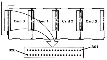
RAM is contained on cards; each card has 128 KB (or more) of storage. A maximum
of four cards can be installed in the system (without using a cable).
Maxing Out the Memory (from Don Hills, edited)
System memory was 640 KB max, with 256 KB as well as 128 KB cards. Any
combination could be used up to 640 KB. To reach 640K with 128K cards, several
people built a short ribbon cable to extend the last card's end connector to
another 128 KB card which they laid on top of the others under the
keyboard.
That was too tight for my liking, so I actually ran the ribbon cable through
to the modem slot and put the 5th card there.
640K is a hardware limit. Any addresses above 640 KB weren't passed to the
memory cards, they were placed on the bus instead for devices like the CGA
video memory.
Memory Cards
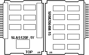
IBM 128KB Memory Card (#4005)
![Board [P]](/other/img/photo.gif)
![Box [P]](/other/img/photo.gif)

This card uses 16x SRM2064M-15 chips for 128K total.
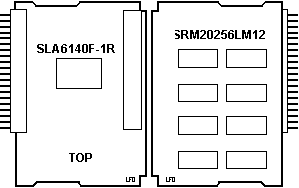
IBM 256KB Memory Card (#6030)
![Board [P]](/other/img/photo.gif)
![Box [P]](/other/img/photo.gif)

This card uses 8x SRM20256M-12 chips for 256K total.
STB 384KB Memory Card "C-RAM 384 (TM)"
![Front [P]](/other/img/photo.gif)
![Back [P]](/other/img/photo.gif)
![Box [P]](/other/img/photo.gif)
![InfoWorld Article [P]](/other/img/photo.gif)

|
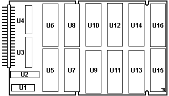
U1 74HC139
U2 "C-RAM" PAL?
U3 74HC373
U4 74HC245
U5-16 32Kx8 SRAM
|
U5-16 12x 32Kx8 SRAM - KM62256ALP-10,
NCR 26C256L-10, or compatible for 384K total.
No components on the solder side, only rubber feet to support the board.
System Board RAM Connector Pinout

| Pin | Signal Name | Dir | |
Pin | Signal Name | Dir |
|---|
| A01 | Address/Data Bit 0 | I/O |
B01 | Address Bit 10 | O |
| A02 | Address/Data Bit 1 | I/O |
B02 | Ground | — |
| A03 | Address/Data Bit 2 | I/O |
B03 | Address Bit 11 | O |
| A04 | +5Vdc | — |
B04 | Ground | — |
| A05 | Address/Data Bit 3 | I/O |
B05 | Address Bit 12 | O |
| A06 | Address/Data Bit 4 | I/O |
B06 | Ground | — |
| A07 | Address/Data Bit 5 | I/O |
B07 | Address Bit 13 | O |
| A08 | +5Vdc | — |
B08 | Ground | — |
| A09 | Address/Data Bit 6 | I/O |
B09 | Address Bit 14 | O |
| A10 | Address/Data Bit 7 | I/O |
B10 | Ground | — |
| A11 | Address Bit 8 | O |
B11 | Address Bit 15 | O |
| A12 | +5Vdc | — |
B12 | Ground | — |
| A13 | Address Bit 9 | O |
B13 | Address Bit 16 | O |
| A14 | Address Latch Enable | O |
B14 | Ground | — |
| A15 | Reserved | ? |
B15 | -Memory Write | O |
| A16 | +5Vdc | — |
B16 | -Data Enable | O |
| A17 | -Memory Card Select 0 | O |
B17 | -Memory Card Select 1 | O |
| A18 | -Memory Card Select 2 | O |
B18 | Ground | — |
| A19 | -Memory Card Select 3 | O |
B19 | RAM Enable | O |
| A20 | -Memory Card Select 4 | O |
B20 | Ground | — |
Address/Data Bit 0 – 7
These multiplexed lines are used to form either the low-order bits of an
address or a byte of data. At the falling edge of the Address Latch Enable
signal, the RAM cards access these eight lines along with lines Address Bit 8
through Address Bit 16 to form an address. At the low level of either Memory
Read or Memory Write, the RAM cards access these eight lines to form a data
byte. The least significant bit is Address/Data Bit 0.
Address Bit 8 – 16
These lines are used to address memory and I/O devices within the system.
The data on these lines is valid through the entire bus cycle.
Memory Card Select 0 – 4
These lines are used to select the card to be accessed. These lines are
shifted at the output of the RAM cards.
Address Latch Enable
This line is used to indicate that the address/data bus contains a valid
address.
Memory Write
This line is used to instruct a RAM card to store the data present on the
data bus.
Data Enable
This line indicates when data should be gated onto the multiplexed
address/data bus.
RAM Enable
This line enables the RAM card to be accessed. When this line is low, all
other signals to the card are ignored.
|